TN2640N3-GP013 데이터 시트보기 (PDF) - Supertex Inc
부품명
상세내역
제조사
TN2640N3-GP013 Datasheet PDF : 8 Pages
| |||
Supertex inc.
TN2640
N-Channel Enhancement-Mode
Vertical DMOS FETs
Features
►►Low threshold (2.0V max.)
►►High input impedance
►►Low input capacitance
►►Fast switching speeds
►►Low on-resistance
►►Free from secondary breakdown
►►Low input and output leakage
Applications
►►Logic level interfaces - ideal for TTL and CMOS
►►Solid state relays
►►Battery operated systems
►►Photo voltaic drives
►►Analog switches
►►General purpose line drivers
►►Telecom switches
General Description
This low threshold enhancement-mode (normally-off)
transistor utilizes a vertical DMOS structure and Supertex’s
well-proven silicon-gate manufacturing process. This
combination produces a device with the power handling
capabilities of bipolar transistors and with the high input
impedance and positive temperature coefficient inherent
in MOS devices. Characteristic of all MOS structures, this
device is free from thermal runaway and thermally induced
secondary breakdown.
Supertex’s vertical DMOS FETs are ideally suited to a
wide range of switching and amplifying applications where
very low threshold voltage, high breakdown voltage, high
input impedance, low input capacitance, and fast switching
speeds are desired.
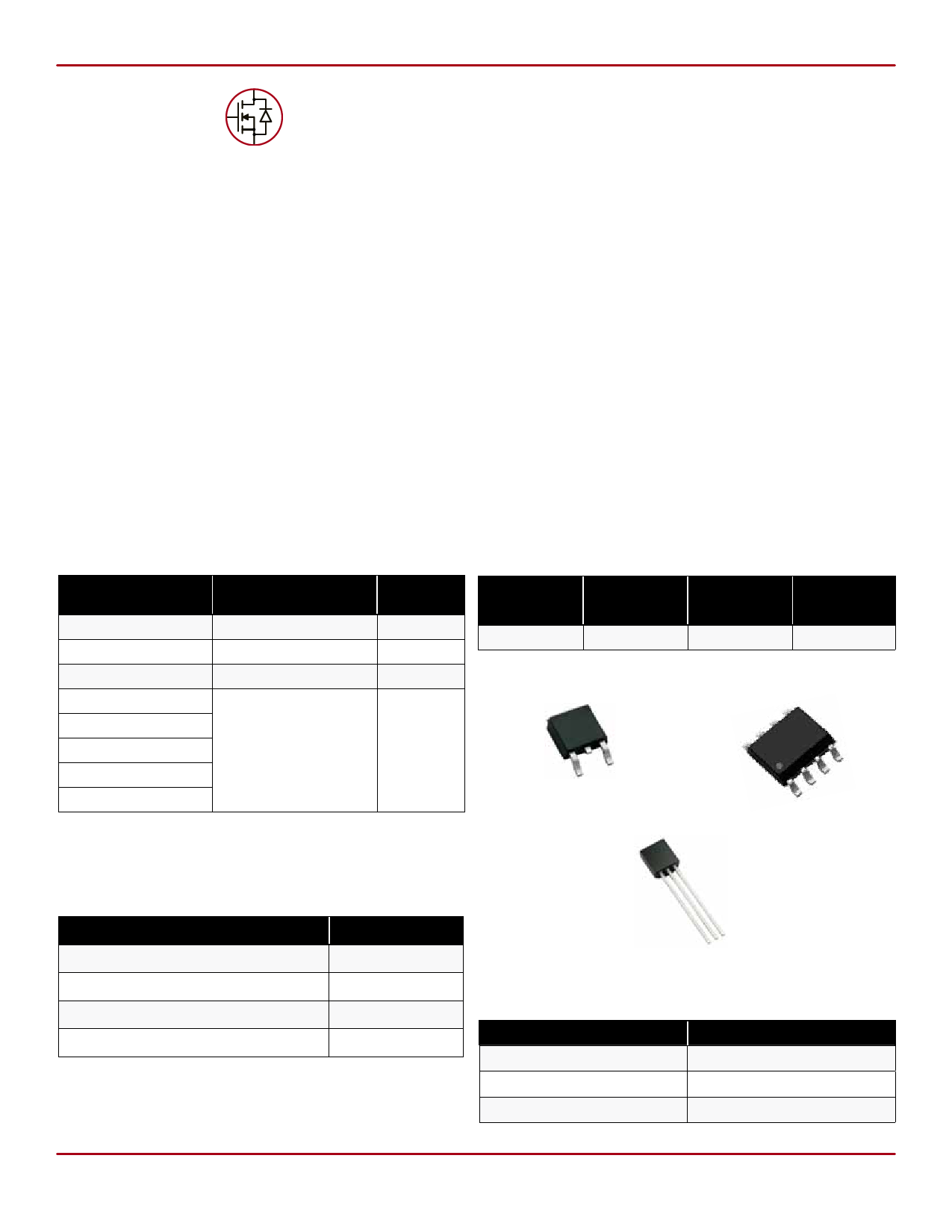
Ordering Information
Part Number
Package Option
Packing
TN2640K4-G
TO-252 (D-PAK)
2000/Reel
TN2640LG-G
8-Lead SOIC
2500/Reel
TN2640N3-G
3-Lead TO-92
1000/Bag
TN2640N3-G P002
TN2640N3-G P003
TN2640N3-G P005 3-Lead TO-92
2000/Reel
TN2640N3-G P013
TN2640N3-G P015
For packaged products, -G indicates package is RoHS compliant (‘Green’).
TO-92 taping specifications and winding styles per EIA-468 Standard.
Devices in Wafer / Die form are RoHS compliant (‘Green’).
Refer to Die Specification VF57 for layout and dimensions.
Product Summary
BVDSS/BVDGS
RDS(ON)
(max)
400V
5.0Ω
Pin Configuration
DRAIN
SOURCE
GATE
TO-252 (D-PAK)
ID(ON)
(min)
2.0A
VGS(th)
(max)
2.0V
DRAIN
DRAIN
DRAIN
DRAIN
GATE
SOURCE
N/C
N/C
8-Lead SOIC
Absolute Maximum Ratings
Parameter
Value
Drain-to-source voltage
Drain-to-gate voltage
Gate-to-source voltage
BVDSS
BVDGS
±20V
Operating and storage temperature -55°C to +150°C
Absolute Maximum Ratings are those values beyond which damage to the device
may occur. Functional operation under these conditions is not implied. Continuous
operation of the device at the absolute rating level may affect device reliability. All
voltages are referenced to device ground.
SOURCE
DRAIN
GATE
TO-92
Typical Thermal Resistance
Package
TO-252 (D-PAK)
θja
81OC/W
8-Lead SOIC
101OC/W
TO-92
132OC/W
Doc.# DSFP-TN2640
C071913
Supertex inc.
www.supertex.com
Share Link: 