MCZ33291EG 데이터 시트보기 (PDF) - Freescale Semiconductor
부품명
상세내역
제조사
MCZ33291EG Datasheet PDF : 27 Pages
| |||
ELECTRICAL CHARACTERISTICS
ELECTRICAL PERFORMANCE CURVES
SCLK
tR (SI)
< 50 ns
0.7 VDD
50%
tDLY(LH)
SO
(Low-to-High)
SO
(High-to-Low)
0.2 VDD
tVALID
0.7 VDD
tR (SO)
tF (SO)
tDLY(HL)
tF (SI)
< 50 ns
5.0 V
0.7 VDD
0.2 VDD 0
VOH
VOL
0.2 VDD
VOH
VOL
SO (Low-to-High) is for an output with internal conditions such that
the low-to-high transition of CS causes the SO output to switch from
high to low.
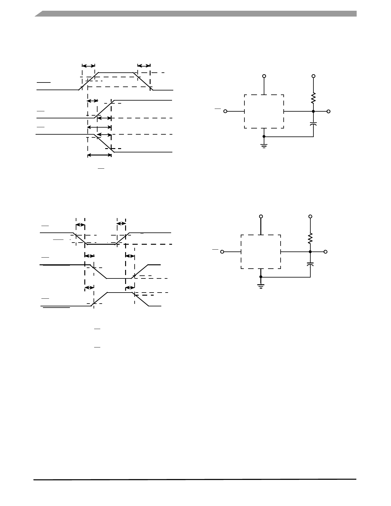
Figure 7. Valid Data Delay Time and
Valid Time Waveforms
CS
0.2 VDD
tR(SI)
< 50 ns
90%
10%
tF(SI)
< 50 ns
0.7 VDD
5.0 V
0
SO
(High-to-Low)
SO
(Low-to-High)
tSO(EN)
90%
tSO(EN)
10%
tSO(DIS)
VTri-State
10%
tSO(DIS)
90%
tSO(DIS)
VOH
VTri-State
1. SO (high-to-low) waveform is for SO output with internal conditions such
that SO output is low except when an output is disabled as a result of de-
tecting a circuit fault with CS in a High Logic state; e.g., open load.
2. SO (low-to-high) waveform is for SO output with internal conditions such
that SO output is high except when an output is disabled as a result of de-
tecting a circuit fault with CS in a High Logic state; e.g., shortened load.
Figure 8. Enable and Disable Time Waveforms
VDD = 5.0 V
VPWR = 14 V
33291
CS
Under
Test
RL = 26 Ω
Output
CL
CL represents the total capacitance of the test fixture and probe.
Figure 9. Switching Time Test Circuit
VDD = 5.0 V
VPWR = 11 V
33291
CS
Under
Test
ΙL = 2.0 Α
(Ουτπυτ ΟΝ)
Output
CL = 20 pF
CL represents the total capacitance of the test fixture and probe.
Figure 10. Output Fault Unlatch Disable
Delay Test Circuit
33291
10
Analog Integrated Circuit Device Data
Freescale Semiconductor
Share Link: 