49LF002 데이터 시트보기 (PDF) - Silicon Storage Technology
부품명
상세내역
제조사
49LF002 Datasheet PDF : 36 Pages
| |||
2 Mbit / 3 Mbit / 4 Mbit / 8 Mbit Firmware Hub
SST49LF002A / SST49LF003A / SST49LF004A / SST49LF008A
Advance Information
Write Operation Status Detection
The SST49LF00xA device provides two software means to
detect the completion of a Write (Program or Erase) cycle,
in order to optimize the system write cycle time. The soft-
ware detection includes two status bits: Data# Polling
(DQ7) and Toggle Bit (DQ6). The End-of-Write detection
mode is incorporated into the FWH Read Cycle. The actual
completion of the nonvolatile write is asynchronous with the
system; therefore, either a Data# Polling or Toggle Bit read
may be simultaneous with the completion of the Write
cycle. If this occurs, the system may possibly get an errone-
ous result, i.e., valid data may appear to conflict with either
DQ7 or DQ6. In order to prevent spurious rejection, if an
erroneous result occurs, the software routine should
include a loop to read the accessed location an additional
two (2) times. If both reads are valid, then the device has
completed the Write cycle, otherwise the rejection is valid.
Data# Polling (DQ7)
When the SST49LF00xA device is in the internal Program
operation, any attempt to read DQ7 will produce the com-
plement of the true data. Once the Program operation is
completed, DQ7 will produce true data. Note that even
though DQ7 may have valid data immediately following the
completion of an internal Write operation, the remaining
data outputs may still be invalid: valid data on the entire
data bus will appear in subsequent successive Read
cycles. During internal Erase operation, any attempt to
read DQ7 will produce a ‘0’. Once the internal Erase opera-
tion is completed, DQ7 will produce a ‘1’. Proper status will
not be given using Data# Polling if the address is in the
invalid range.
Toggle Bit (DQ6)
During the internal Program or Erase operation, any con-
secutive attempts to read DQ6 will produce alternating
‘0’s and ‘1’s, i.e., toggling between 0 and 1. When the
internal Program or Erase operation is completed, the
toggling will stop.
Multiple Device Selection
The four ID pins, ID[3:0], allow multiple devices to be
attached to the same bus by using different ID strapping in
a system. When the SST49LF00xA is used as a boot
device, ID[3:0] must be strapped as 0000, all subsequent
devices should use a sequential up-count strapping (i.e.
0001, 0010, 0011, etc.). The SST49LF00xA will compare
the strapping values, if there is a mismatch, the device will
ignore the remainder of the cycle and go into standby
mode. For further information regarding FWH device map-
ping and paging, please refer to the Intel 82801(ICH) I/O
Controller Hub documentation. Since there is no ID support
in PP Mode, to program multiple devices a stand-alone
PROM programmer is recommended.
REGISTERS
There are three types of registers available on the
SST49LF00xA, the General Purpose Inputs Register,
Block Locking Registers and the JEDEC ID Registers.
These registers appear at their respective address location
in the 4 GByte system memory map. Unused register loca-
tions will read as 00H. Any attempt to read or write any reg-
isters during internal Write operation will be ignored.
General Purpose Inputs Register
The GPI_REG (General Purpose Inputs Register) passes
the state of FGPI[4:0] pins at power-up on the
SST49LF00xA. It is recommended that the FGPI[4:0] pins
are in the desired state before FWH4 is brought low for the
beginning of the bus cycle, and remain in that state until the
end of the cycle. There is no default value since this is a
pass-through register. The GPI register for the boot device
appears at FFBC0100H in the 4 GByte system memory
map, and will appear elsewhere if the device is not the boot
device. Register is not available for read when the device is
in Erase/Program operation. See Table 3 for the GPI_REG
bits and function.
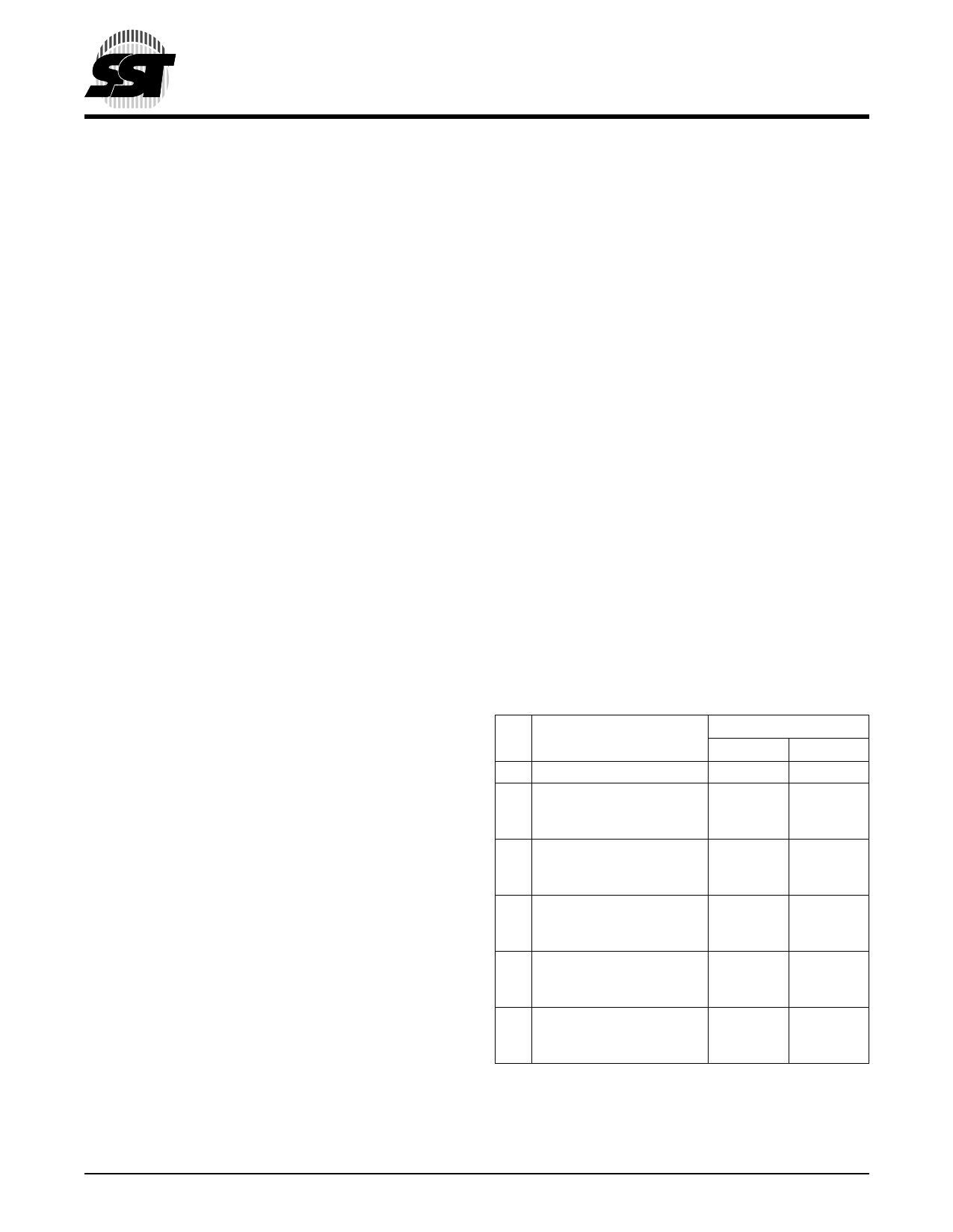
TABLE 3: GENERAL PURPOSE INPUTS REGISTER
Pin #
Bit
Function
7:5 Reserved
4 FGPI[4]
Reads status of general
purpose input pin
3 FGPI[3]
Reads status of general
purpose input pin
2 FGPI[2]
Reads status of general
purpose input pin
1 FGPI[1]
Reads status of general
purpose input pin
0 FGPI[0]
Reads status of general
purpose input pin
32-PLCC
-
30
32-TSOP
-
6
3
11
4
12
5
13
6
14
T3.2 504
©2001 Silicon Storage Technology, Inc.
6
S71161-06-000 9/01 504
Share Link: 