HT45FM03B(2009) 데이터 시트보기 (PDF) - Holtek Semiconductor
부품명
상세내역
제조사
HT45FM03B Datasheet PDF : 83 Pages
| |||
HT45FM03B
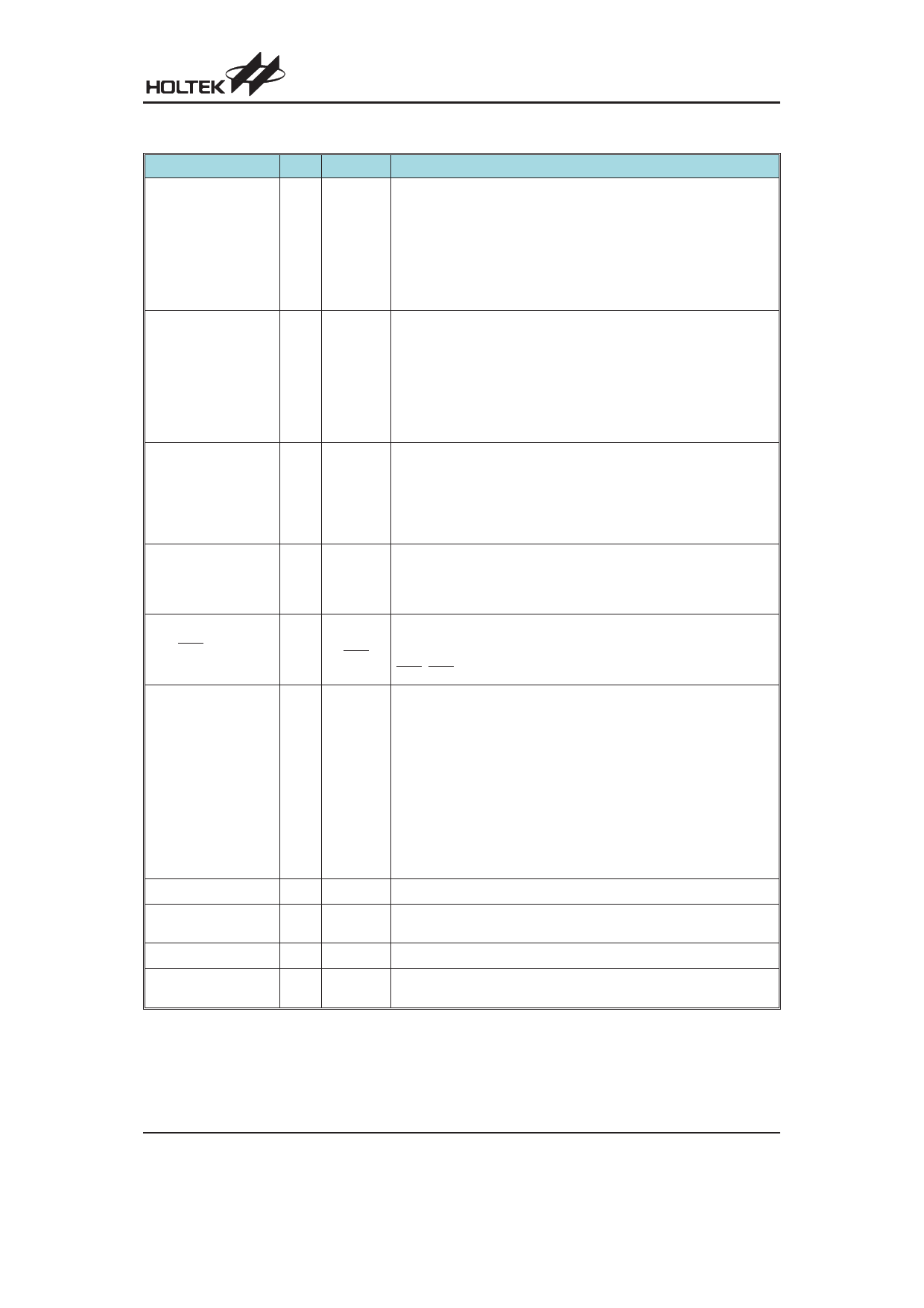
Pad Description
Pad Name
I/O
PA0/OPVINP
PA1/CVINP
PA2/CVINN
PA3/COUT
PA4/INT0A
I/O
PA5/INT0B
PA6/INT0C
PA7/INT1
PB0/AN0
PB1/AN1
PB2/AN2/OPOUT
PB3/AN3/OPVINN
PB4/AN4/INT0A
I/O
PB5/AN5/INT0B
PB6/AN6/INT0C
PB7/AN7/TMR0/TMR1
PC0/PWM0H
PC1/PWM0L
PC2/PWM1H
PC3/PWM1L
I/O
PC4/PWM2H
PC5/PWM2L
PD0/PFD
I/O
PD1/RES
I/O
PD2/OSC1
PD3/OSC2
I/O
VSS
¾
AVSS
¾
VDD
¾
AVDD
¾
Option
Description
Pull-high
Wake-up
INT0A
INT0B
INT0C
Bidirectional 8-bit input/output port. Each pin can be configured as
wake-up input by configuration option. Software instructions determine
if the pin is a CMOS output or Schmitt Trigger input. Configuration op-
tions determine if the pins have pull-high resistors. Pins PA4~PA6 are
pin-shared with INT0A, INT0B and INT0C, the function being selected
via configuration options. PA7 is pin-shared with the external interrupt
pin INT1. PA1, PA2 and PA3 are pin-shared with comparator pins
CVINP, CVINN and COUT. PA0 is shared with OPVINP.
Pull-high
INT0A
INT0B
INT0C
Bidirectional 8-bit input/output port. Software instructions determine if
the pin is a CMOS output or Schmitt Trigger input. Configuration op-
tions determine if the pins have pull-high resistors. PB is pin-shared
with the A/D inputs. Pins PB4~PB6 are also pin-shared with INT0A,
INT0B and INT0C, the function being selected via configuration op-
tions. Pins PB2 and PB3 are also pin pin-shared with operational am-
plifier pins OPOUT and OPVINN. Pin PB7 is also pin-shared with timer
input pins TMR0 and TMR1.
Pull-high
Bidirectional 6-bit input/output port. Software instructions determine if
the pin is a CMOS output or Schmitt Trigger input. Configuration op-
tions determine if the pins have pull-high resistors. PC is pin shared
with the Pulse Width Modulation complimentary output pairs,
PWM0H~PWM2H and PWM0L~PWM2L.
Pull-high
PFD
Bidirectional 1-line I/O. Software instructions determine if the pin is a
CMOS output or Schmitt Trigger input. A configuration option deter-
mines if pin PD0 has a pull-high resistor. Pin PD0 is shared with the
PFD output.
PD1 or
RES
Bidirectional 1-bit input/output port. Software instructions determine if
the pin is a CMOS output or Schmitt Trigger input. Pin PD1 does not
have a pull-high option. Pin PD1 is pin-shared with the reset input pin
RES. RES is a Schmitt Trigger reset input. Active low.
1.Int. RC
OSC
2.Crystal
OSC
3.Ext. RC
OSC
Bidirectional 2-line I/O. Software instructions determine if the pins are
CMOS outputs or Schmitt Trigger inputs. Pin PD2~PD3 do not have
pull-high options. Configuration options determine if the pins are to be
used as oscillator pins or I/O pins. Configuration options also deter-
mine which oscillator mode is selected. The three oscillator modes are:
1. Internal RC OSC: both pins configured as I/Os.
2. External crystal OSC: both pins configured as OSC1/OSC2.
3. External RC OSC+PD3: PD2 is configured as OSC1 pin, PD3 con-
figured as an I/O.
If the internal RC OSC is selected, the frequency will be fixed at either
12MHz, 16MHz or 20MHz, dependent upon which configuration option
is chosen.
¾
Negative power supply, ground
¾
Ground connection for A/D converter. The VSS and AVSS are the
same pin at 28 pin package.
¾
Positive power supply
¾
Power supply connection for A/D converter. The VDD and AVDD are
the same pin at 28 pin package.
Rev. 1.00
3
December 16, 2009
Share Link: 