LH28F008SCT-V12 데이터 시트보기 (PDF) - Sharp Electronics
부품명
상세내역
제조사
LH28F008SCT-V12 Datasheet PDF : 40 Pages
| |||
to read data from, or write data to any other flash
memory array location.
Individual block locking uses a combination of bits,
sixteen block lock-bits and a master lock-bit, to lock
and unlock blocks. Block lock-bits gate block erase
and byte write operations, while the master lock-bit
gates block lock-bit modification. Lock-bit
configuration operations (Set Block Lock-Bit, Set
Master Lock-Bit, and Clear Block Lock-Bits
commands) set and cleared lock-bits.
The status register indicates when the WSM’s block
erase, byte write, or lock-bit configuration operation
is finished.
The RY/BY# output gives an additional indicator of
WSM activity by providing both a hardware signal
of status (versus software polling) and status
masking (interrupt masking for background block
erase, for example). Status polling using RY/BY#
minimizes both CPU overhead and system power
consumption. When low, RY/BY# indicates that the
WSM is performing a block erase, byte write, or
lock-bit configuration. RY/BY#-high indicates that
the WSM is ready for a new command, block erase
is suspended (and byte write is inactive), byte write
is suspended, or the device is in deep power-down
mode.
The access time is 85 ns (tAVQV) at the VCC supply
voltage range of 4.75 to 5.25 V over the
temperature range, 0 to +70˚C (LH28F008SC-V)/
–25 to +85˚C (LH28F008SCH-V). At 4.5 to 5.5 V
VCC, the access time is 90 ns or 120 ns.
The Automatic Power Saving (APS) feature
substantially reduces active current when the
device is in static mode (addresses not switching).
In APS mode, the typical ICCR current is 1 mA at
5 V VCC.
LH28F008SC-V/SCH-V
When CE# and RP# pins are at VCC, the ICC
CMOS standby mode is enabled. When the RP#
pin is at GND, deep power-down mode is enabled
which minimizes power consumption and provides
write protection during reset. A reset time (tPHQV) is
required from RP# switching high until outputs are
valid. Likewise, the device has a wake time (tPHEL)
from RP#-high until writes to the CUI are
recognized. With RP# at GND, the WSM is reset
and the status register is cleared.
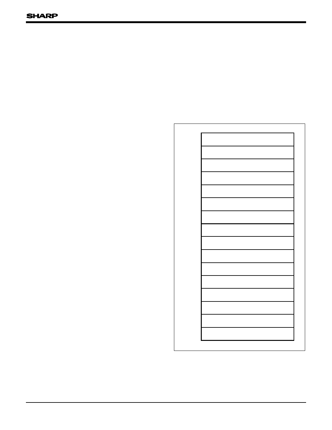
FFFFF
F0000
EFFFF
E0000
DFFFF
D0000
CFFFF
C0000
BFFFF
B0000
AFFFF
A0000
9FFFF
90000
8FFFF
80000
7FFFF
70000
6FFFF
60000
5FFFF
50000
4FFFF
40000
3FFFF
30000
2FFFF
20000
1FFFF
10000
0FFFF
00000
64 k-Byte Block
15
64 k-Byte Block
14
64 k-Byte Block
13
64 k-Byte Block
12
64 k-Byte Block
11
64 k-Byte Block
10
64 k-Byte Block
9
64 k-Byte Block
8
64 k-Byte Block
7
64 k-Byte Block
6
64 k-Byte Block
5
64 k-Byte Block
4
64 k-Byte Block
3
64 k-Byte Block
2
64 k-Byte Block
1
64 k-Byte Block
0
Fig. 1 Memory Map
-6-
Share Link: 