M52348FP 데이터 시트보기 (PDF) - MITSUBISHI ELECTRIC
부품명
상세내역
제조사
M52348FP Datasheet PDF : 11 Pages
| |||
MITSUBISHI ICs (Monitor)
M52348FP
WIDE FREQUENCY BAND ANALOG SWITCH
CAUTIONS FOR USING THE IC
1. Standard video inputs for R, G and B are specified to be 0.7 VP-P.
2. The H and V inputs are specified to be 5.0 VTTL.
3. Input signals into input pins at fully lowered impedance.
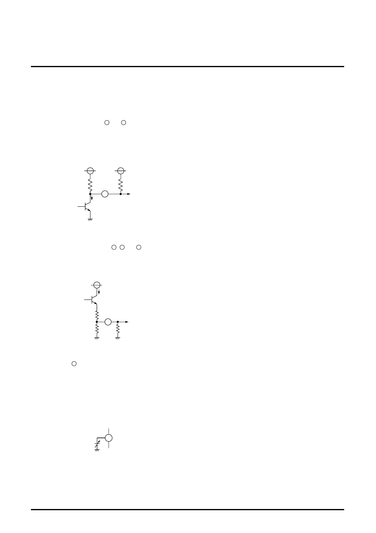
4. The H and V output pins (pins 21 and 22 ) are as shown in Figure
1. Resistance can be inserted into a portion between power
supplies to improve the rising speed. However, set the R value
to limit the current to 7.5 mA or less. In Figure 1, R is 2 kΩ or
more.
5V
5V
1kΩ
R
CAUTIONS FOR MANUFACTURING BOARDS
Built-in wide band analog switch may cause oscillation due to the
wiring shape on the board. Be careful for the following points.
• When inserting an output pull-down resistance, make wire
between the output pin and the resistance as short as possible.
• Make the load capacitance of output pins as small as possible.
• Install the Vcc-GND bus controller capacitance near the pin.
• Vcc shall use a stable power supply. (Individual Vcc should use
an independent power supply.)
• Insertion of a resistance of several tens of Ω between the output
pin and the circuit at the next stage makes oscillation harder.
• GND should be as wide as possible. Basically, solid earth should
be used.
I=7.5 mA or less
Fig. 1
5. The R, G and B output pins (pins 27 , 30 and 35 ) are as shown in
Figure 2. Pull-down resistance can be added to between GNDs
according to the driving capability. However, set the R value to
limit current I to 10 mA or less. In Figure 2, R is 500Ω or more.
5V
I=10 mA or less
50Ω
430kΩ
R
Fig. 2
6. The switch (pin 19 ) can be switched with GND and OPEN.
GND: Outputs signal from the INPUT 1 side.
OPEN: Outputs signal from the INPUT 2 side.
For switching by applying voltage as shown in Figure 3;
0 to 0.5V: Outputs signal from INPUT 1 side.
2 to 5V: Outputs signal from INPUT 2 side.
The applied voltage shall be less than Vcc.
19
Fig. 3
10
Share Link: 