M52342FP 데이터 시트보기 (PDF) - Renesas Electronics
부품명
상세내역
제조사
M52342FP Datasheet PDF : 19 Pages
| |||

M52342FP
VIN MIN Input sensitivity
Input SG4 (Vi = 90 dBµ) into VIF IN, and then gradually reduce Vi and measure the input level when the 20 kHz
component of EQ output TP22A reaches −3 dB from VO det level.
VIN MAX Maximum Allowable Input
1. Input SG5 (Vi = 90 dBµ) into VIF IN, and measure the level of the 20 kHz component of EQ output.
2. Gradually increase the Vi of SG and measure the input level when the output reaches −3 dB.
GR AGC Control Range
GR = VIN MAX − VIN MIN (dB)
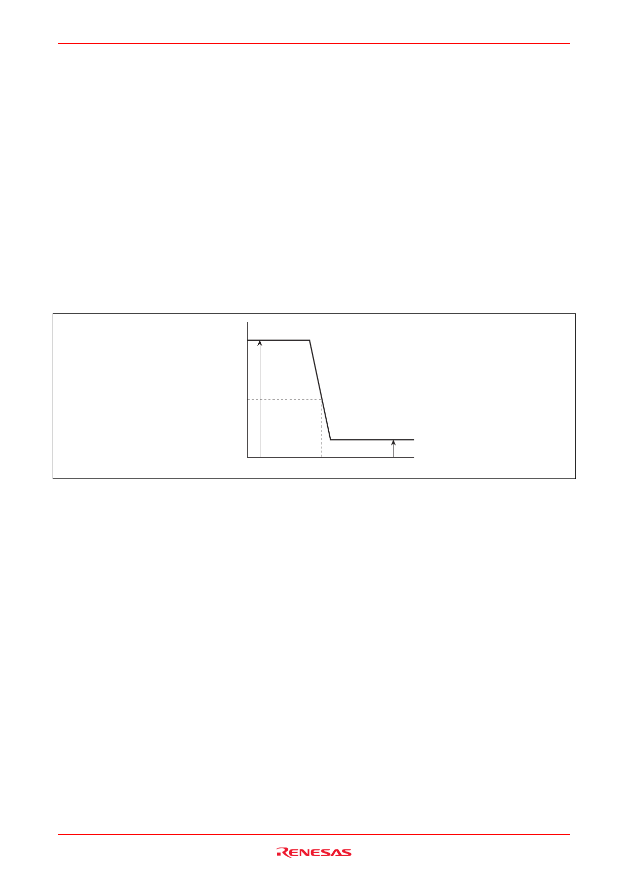
V3 RF AGC Operating Voltage
Input SG8 into VIF IN, and gradually reduce Vi and then measure the input level when RF AGC output TP3 reaches
1/2 VCC, as shown below.
TP3
Voltage
V3H
1/2 VCC
V3L
Vi
Vi (dBµ)
CL-U Capture Range
1. Increase the frequency of SG9 until the VCO is out of locked-oscillation.
2. Decrease the frequency of SG9 and measure the frequency fU when the VCO locks.
CL-U = fU − 58.75 (MHz)
CL-L Capture Range
1. Decrease the frequency of SG9 until the VCO is out of locked-oscillation.
2. Increase the frequency of SG9 and measure the frequency fL when the VCO locks.
CL-L = 58.75 − fL (MHz)
CL-T Capture Range
CL-T = CL-U + CL-L (MHz)
Rev.2.00 Jun 14, 2006 page 7 of 18