M61316SP 데이터 시트보기 (PDF) - Renesas Electronics
부품명
상세내역
제조사
M61316SP Datasheet PDF : 27 Pages
| |||
M61311SP/M61316SP
Electrical Characteristics Test Method
ICC1 5 V Circuit Current1 Power Save Mode
Measuring conditions are as listed in supplementary Table. Measured with a current meter at test point IB.
ICC2 12 V Circuit Current2 Normal Mode
Measuring conditions are as listed in supplementary Table. Measured with a current meter at test point IA.
ICC3 5 V Circuit Current3 Normal Mode
Measuring conditions are as listed in supplementary Table. Measured with a current meter at test point IB.
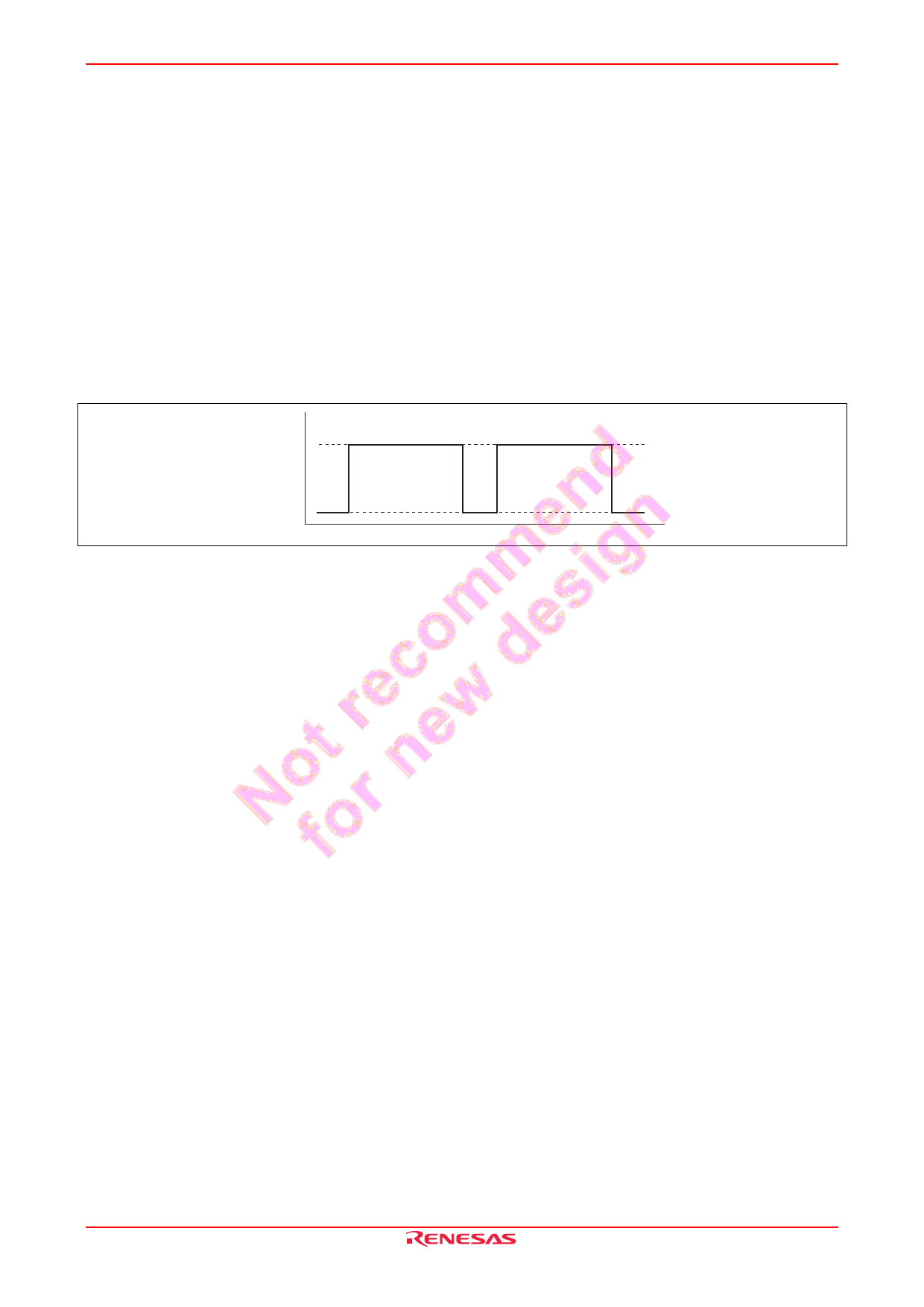
Vomax Output Dynamic Range
It makes the amplitude of SG1 1.4 P-P. Measure the DC voltage of the white level of the waveform output.
The measured value is called Vomax.
(VDC)
Vomax
Waveform output
0.5
0.0
Vimax Maximum Input
Increase the input signal (SG1) amplitude gradually, starting from 0.7 VP-P. Measure the amplitude of the input signal
when the output signal starts becoming distorted.
GV Maximum Gain
Input SG1, and measure the amplitude output at OUT (26, 28, 30). The amplitude is called VOUT (26, 28, 30).
Maximum gain GV is calculated by the equation below:
GV = 20log (VOUT / 0.7) (dB)
∆GV Relative Maximum Gain
Relative maximum gain ∆GV is calculated by the equation below:
∆GV = VOUT (26) / VOUT (28),
VOUT (28) / VOUT (30),
VOUT (30) / VOUT (26)
VC1 Main Contrast Control Characteristics1 (Max.)
Input SG1, and measure the amplitude output at OUT (26, 28, 30). The amplitude is called VOUT (26, 28, 30).
The measured value is called VC1.
∆VC1 Main Contrast Control Relative Characteristics1
Relative characteristics ∆VC1 is calculated by the equation below:
∆VC1 = VOUT (26) / VOUT (28),
VOUT (28) / VOUT (30),
VOUT (30) / VOUT (26)
REJ03F0199-0201 Rev.2.01 Mar 31, 2008
Page 9 of 26
Share Link: 