MAX9736 데이터 시트보기 (PDF) - Maxim Integrated
부품명
상세내역
제조사
MAX9736 Datasheet PDF : 25 Pages
| |||
Mono/Stereo High-Power Class D Amplifier
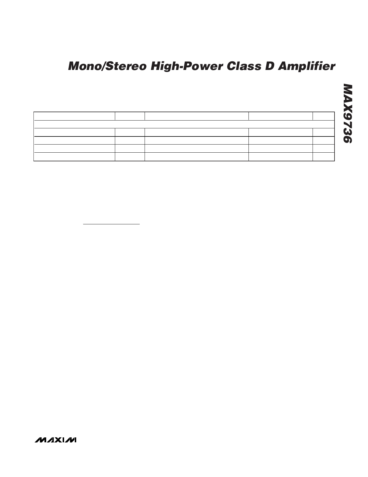
ELECTRICAL CHARACTERISTICS (continued)
(VPVDD = 20V, VVS = 5V, VAGND = VPGND = 0V, VMOD = VSHDN = VMUTE = 5V, REGEN = MONO = AGND, C1 = 0.1μF, C2 = 1μF,
RIN_ = 20kΩ and RFB_= 20kΩ, RL = ∞, AC measurement bandwidth 22Hz to 22kHz, TA = TMIN to TMAX, unless otherwise noted.
Typical values are at TA = +25°C.) (Notes 4, 5)
PARAMETER
SYMBOL
CONDITIONS
MIN TYP MAX UNITS
DIGITAL INTERFACE
Input Voltage High
Input Voltage Low
Input Voltage Hysteresis
VINH
VINL
2
V
0.8
V
50
mV
Input Leakage Current
±10
μA
Note 4:
Note 5:
Note 6:
Note 7:
Note 8:
All devices are 100% production tested at +25°C. All temperature limits are guaranteed by design.
Stereo mode (MONO = GND) specified with 8Ω resistive load in series with a 68μH inductive load connected across BTL
outputs. Mono mode (MONO = 5V) specified with a 4Ω resistive load in series with a 33μH inductive load connected
across BTL outputs.
Output swing is specified with respect to VCOM.
For typical applications, an external 5V supply is not required. Therefore, set REGEN = 5V. If thermal performance is a
concern, set REGEN = 0V and provide an external regulated 5V supply.
Output amplifier gain is defined as:
20
×
⎛
log⎝⎜
|
(VOUT_+ ) − (VOUT
| VFB _ |
_−
)
|
⎞
⎠⎟
Note 9: Amplifier inputs AC-coupled to GND.
Note 10: Specified at room temperature with an 8Ω resistive load in series with a 68μH inductive load connected across BTL outputs.
Mode transitions controlled by SHDN control pin.
_______________________________________________________________________________________ 5
Share Link: 