MCP6546 데이터 시트보기 (PDF) - Microchip Technology
부품명
상세내역
제조사
MCP6546 Datasheet PDF : 32 Pages
| |||
MCP6546/6R/6U/7/8/9
1.0 ELECTRICAL
CHARACTERISTICS
Absolute Maximum Ratings †
VDD - VSS .........................................................................7.0V
Open-Drain output............................................... VSS + 10.5V
Analog Input (VIN+, VIN-)††............. VSS - 1.0V to VDD + 1.0V
All other inputs and outputs ........... VSS – 0.3V to VDD + 0.3V
Difference Input voltage ...................................... |VDD – VSS|
Output Short-Circuit Current .................................continuous
Current at Input Pins ....................................................±2 mA
Current at Output and Supply Pins ............................±30 mA
Storage temperature .....................................-65°C to +150°C
Maximum Junction Temperature (TJ) .......................... +150°C
ESD protection on all pins:
(HBM;MM) .....................................2 kV;200V (MCP6546U)
(HBM;MM) ................................ 4 kV; 200V (all other parts)
† Notice: Stresses above those listed under “Absolute Maxi-
mum Ratings” may cause permanent damage to the device.
This is a stress rating only and functional operation of the
device at those or any other conditions above those indicated
in the operational listings of this specification is not implied.
Exposure to maximum rating conditions for extended periods
may affect device reliability.
†† See Section 4.1.2 “Input Voltage and Current
Limits”
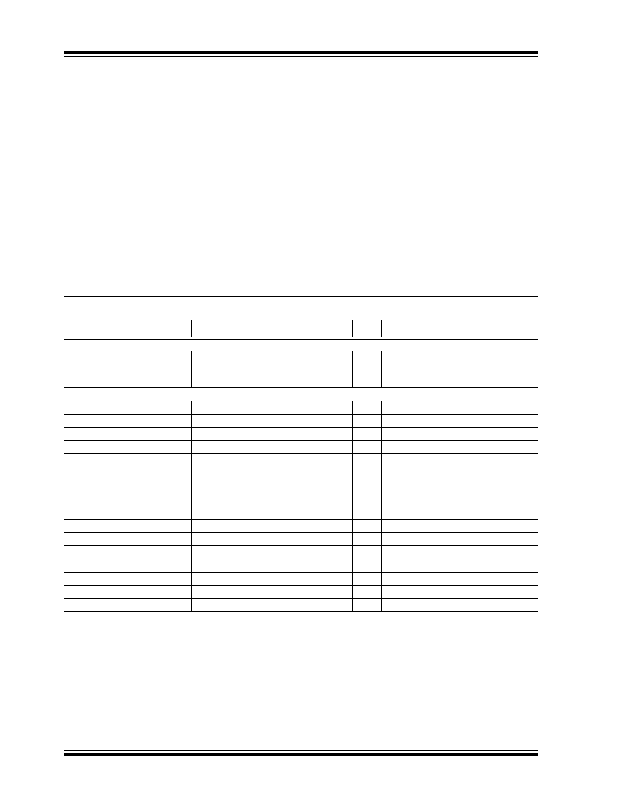
DC CHARACTERISTICS
Electrical Specifications: Unless otherwise indicated, VDD = +1.6V to +5.5V, VSS = GND, TA = 25°C, VIN+ = VDD/2, VIN– = VSS,
RPU = 2.74 kΩ to VPU = VDD (Refer to Figure 1-3).
Parameters
Sym
Min Typ Max Units
Conditions
Power Supply
Supply Voltage
Quiescent Current
(per comparator)
VDD
1.6
—
5.5
V VPU ≥ VDD
IQ
0.3
0.6
1
µA IOUT = 0
Input
Input Voltage Range
VCMR VSS − 0.3 — VDD + 0.3 V
Common Mode Rejection Ratio
CMRR
55
70
—
dB VDD = 5V, VCM = -0.3V to 5.3V
Common Mode Rejection Ratio
CMRR
50
65
—
dB VDD = 5V, VCM = 2.5V to 5.3V
Common Mode Rejection Ratio
CMRR
55
70
—
dB VDD = 5V, VCM = -0.3V to 2.5V
Power Supply Rejection Ratio
PSRR
63
80
—
dB VCM = VSS
Input Offset Voltage
VOS
-7.0
±1.5
+7.0
mV VCM = VSS (Note 1)
Drift with Temperature
ΔVOS/ΔTA
—
±3
—
µV/°C TA = -40°C to +125°C, VCM = VSS
Input Hysteresis Voltage
VHYST
1.5
3.3
6.5
mV VCM = VSS (Note 1)
Linear Temp. Co.
Quadratic Temp. Co.
TC1
—
6.7
—
µV/°C TA = -40°C to +125°C, VCM = VSS (Note 2)
TC2
—
-0.035
—
µV/°C2 TA = -40°C to +125°C, VCM = VSS (Note 2)
Input Bias Current
IB
—
1
—
pA VCM = VSS
At Temperature (I-Temp parts)
IB
—
25
100
pA TA = +85°C, VCM = VSS (Note 3)
At Temperature (E-Temp parts)
IB
—
1200 5000
pA TA = +125°C, VCM = VSS (Note 3)
Input Offset Current
Common Mode Input Impedance
Differential Input Impedance
IOS
ZCM
ZDIFF
—
±1
—
pA VCM = VSS
—
1013||4
—
Ω||pF
—
1013||2
—
Ω||pF
Note 1: The input offset voltage is the center of the input-referred trip points. The input hysteresis is the difference between the
input-referred trip points.
2: VHYST at differential temperatures is estimated using: VHYST (TA) = VHYST + (TA -25°C) TC1 + (TA - 25°C)2TC2.
3: Input bias current at temperature is not tested for the SC-70-5 package
4: Do not short the output above VSS + 10V. Limit the output current to Absolute Maximum Rating of 30 mA. The minimum
VPU test limit was VDD before Dec. 2004 (week code 52).
DS21714E-page 2
© 2006 Microchip Technology Inc.
Share Link: 