STA333ML13TR 데이터 시트보기 (PDF) - STMicroelectronics
부품명
상세내역
제조사
STA333ML13TR
STMicroelectronics

STA333ML13TR Datasheet PDF : 23 Pages
| |||
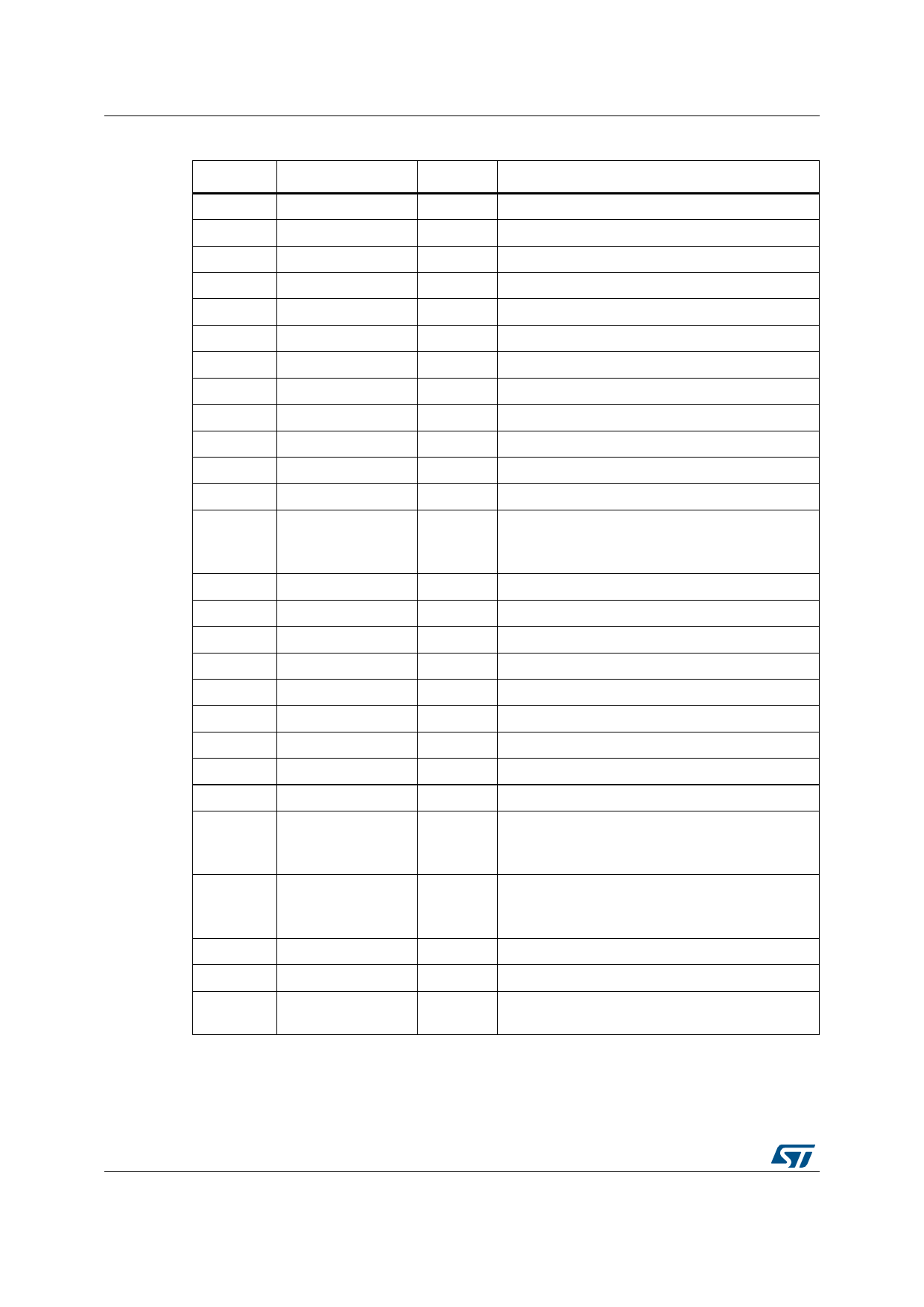
Pin description
Pin
11
12
13
14
15
16
17
18
19
20
21
22
23
24
25
26
27
28
29
30
31
32
33
34
35
36
-
STA333ML
Table 2. Pin description (continued)
Name
Type
Description
VCC1
GND1
OUT1A
GND_REG
Power
Gnd
Out
Analog
Power positive supply
Power negative supply
Output half-bridge 1A
Internal ground reference
VDD_REG
CONFIG
N.C.
N.C.
Analog
In
-
-
Internal 3.3 V reference voltage
Configuration mode, must be connected to ground
Not connected
Not connected
N.C.
N.C.
VDD_DIG
GND_DIG
-
-
Power
Gnd
Not connected
Not connected
Positive supply digital
Digital ground
PWRDN
VDD_PLL
In
Power
Power-down:
0: low-power mode
1: normal operation
Positive supply for PLL
FILTER_PLL
GND_PLL
XTI
BICKI
LRCKI
SDI
RESET
INT_LINE
ONSEL
GAIN
GND_DIG
VDD_DIG
In
Gnd
In
In
In
In
In
Out
In
In
Gnd
Power
Connection to PLL filter
Negative supply for PLL
PLL input clock, 256 * fs or 384 * fs
I2S serial clock
I2S left/right clock
I2S serial data channel
Reset
Fault interrupt
Oversampling selector:
0: 256 * fs
1: 384 * fs
Gain selector:
0: 0 dBFs
1: 24 dBFs
Digital ground
Digital supply
EP
-
Exposed pad for PCB heatsink, to be connected to
ground plane
6/23
DocID13177 Rev 8
Share Link: