MRFIC1817R2 데이터 시트보기 (PDF) - Motorola => Freescale
부품명
상세내역
제조사
MRFIC1817R2 Datasheet PDF : 8 Pages
| |||
Typical Characteristics
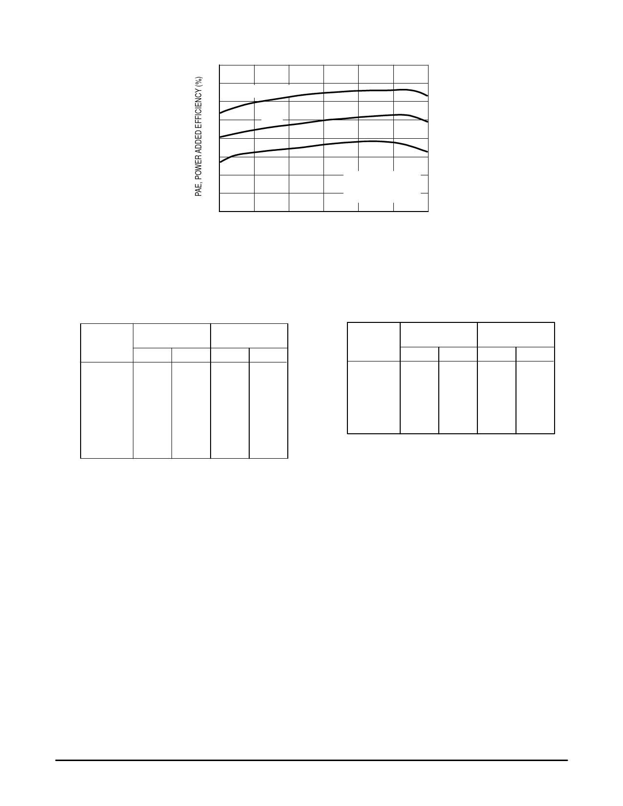
48
46
TA = –35°C
44
42
25°C
40
85°C
38
36
Pin = 5 dBm
34
VD1, VD2, VD3 = 3.6 V
VSS = –4 V
32
1.85
1.86
1.87
1.88
1.89
1.9
1.91
f, FREQUENCY (GHz)
Figure 15. Power Added Efficiency versus
Frequency – PCS Band
Table 1. Optimum Loads Derived from
Circuit Characterization
Zin
ZOL*
OHMS
f
OHMS
MHz
R
jX
R
jX
1710
7.77
–34.15
4.89
9.50
1720
7.84
–34.37
4.87
9.34
1730
7.87
–34.67
4.86
9.18
1740
8.07
–34.79
4.78
8.94
1750
8.24
–35.05
4.77
8.70
1760
8.39
–35.22
4.73
8.51
1770
8.44
–35.56
4.70
8.32
1780
8.52
–35.79
4.67
8.12
1785
8.57
–35.82
4.65
7.95
Zin represents the input impedance of the device.
ZOL* represents the conjugate of the optimum output load to present
to the device.
Table 2. Optimum Loads Derived from
Circuit Characterization – PCS Band
Zin
ZOL*
f
OHMS
OHMS
MHz
R
jX
R
jX
1850
3.97
–39.68
7.49
3.07
1860
3.94
–40.31
7.42
2.81
1870
4.09
–40.65
7.38
2.51
1880
4.04
–40.92
7.31
2.28
1890
4.18
–41.21
7.28
2.02
1900
4.27
–41.48
7.28
1.73
1910
4.26
–41.71
7.23
1.56
Zin represents the input impedance of the device.
ZOL* represents the conjugate of the optimum output load to present
to the device.
MRFIC1817
6
MOTOROLA RF DEVICE DATA
Share Link: 