VDD501MCTA 데이터 시트보기 (PDF) - AnaSem Semiconductors
부품명
상세내역
제조사
VDD501MCTA
AnaSem Semiconductors

VDD501MCTA Datasheet PDF : 20 Pages
| |||
Low voltage, Low power, ±1% High detect accuracy with delay circuit CMOS Voltage Detector
Rev. E13-01
VDD Series
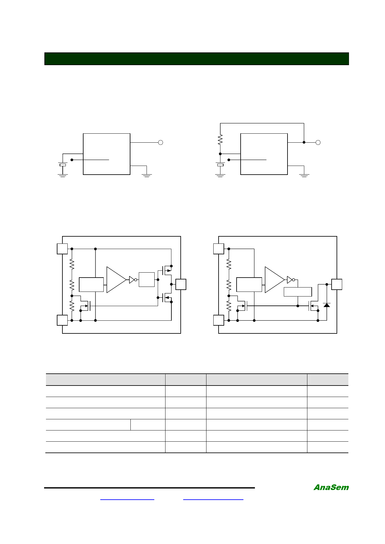
TYPICAL APPLICATION CIRCUITS
CMOS output
N-channel open drain output
VOUT
VIN
VSS
100KΩ
VOUT
VIN
VSS
BLOCK DIAGRAM
CMOS output
VIN
N-channel open drain output
VIN
+
Voltage _
Reference
Vss
Delay
circuit
VOUT
Vss
+
Voltage _
Reference
Delay circuit
VOUT
ABSOLUTE MAXIMUM RATINGS
Items
Symbol
Ratings
Unit
Input voltage range
VIN
–0.3 ~ +7.0
V
Output current
IOUT
50
mA
Output voltage range
VOUT
VSS –0.3 ~ VIN +0.3
V
Power dissipation ※1) SOT-23
PD
400
mW
Operating temperature range
TOPR
–40 ~ +85
°C
Storage temperature range
TSTG
–55 ~ +125
°C
Note :
※1) Power dissipation depends on conditions of mounting on boards.
PCB dimension is 50mm×50mm×1.6mm.
AnaSem
3
www.anasemi.com
sales@anasemi.com
.......... Future of the analog world
Share Link: