MC10E411FN 데이터 시트보기 (PDF) - Motorola => Freescale
부품명
상세내역
제조사
MC10E411FN Datasheet PDF : 6 Pages
| |||
MC10E411
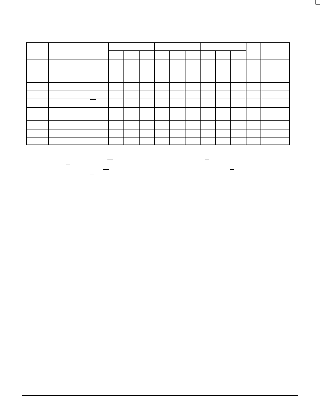
AC CHARACTERISTICS (VEE = VEE (min) to VEE (max); VCC = VCCO = GND)
0°C
25°C
85°C
Symbol
Characteristic
Min Typ Max Min Typ Max Min Typ Max Unit Condition
tPLH
tPHL
Propagation Delay to Output
IN (differential)
400
IN (single-ended)
350
EN to Q
450
600 430
650 380
850 450
630 500
680 450
850 450
ps
700
750
850
Note 1.
Note 2.
ts
tH
tR
tskew
Setup Time
EN to IN 200 0
200 0
200 0
ps
Hold Time
IN to EN 0 –200
0 –200
0 –200
ps
Release Time
EN to IN 300 100
300 100
300 100
ps
Within-Device Skew
Part-to-Part Skew (Diff)
50
50
50 ps
200
200
200
Note 3.
Note 4.
Note 5.
Note 6.
VPP
Minimum Input Swing
250
250
250
mV
Note 7.
VCMR Common Mode Range
–1.6
–0.4 –1.6
–0.4 –1.6
–0.4 V
Note 8.
tr/tf
Output Rise/Fall Time
275
600 275
600 275
600 ps 20%–80%
1. The differential propagation delay is defined as the delay from the crossing points of the differential input signals to the crossing point of the
differential output signals.
2. The single-ended propagation delay is defined as the delay from the 50% point of the input signal to the 50% point of the output signal.
3. The setup time is the minimum time that EN must be asserted prior to the next transition of IN/IN to prevent an output response greater than
±75 mV to that IN/IN transition (see Figure 1).
4. The hold time is the minimum time that EN must remain asserted after a negative going IN or a positive going IN to prevent an output response
greater than ±75 mV to that IN/IN transition (see Figure 2).
5. The release time is the minimum time that EN must be deasserted prior to the next IN/IN transition to ensure an output response that meets
the specified IN to Q propagation delay and output transition times (see Figure 3).
6. The within-device skew is defined as the worst case difference between any two similar delay paths within a single device.
7. VPP(min) is defined as the minimum input differential voltage which will cause no increase in the propagation delay. The VPP(min) is AC limited
for the E411 as a differential input as low as 50 mV will still produce full ECL levels at the output.
8. VCMR is defined as the range within which the VIH level may vary, with the device still meeting the propagation delay specification. The VIL level
must be such that the peak to peak voltage is less than 1.0 V and greater than or equal to VPP(min).
MOTOROLA
2–4
ECLinPS and ECLinPS Lite
DL140 — Rev 4
Share Link: 