M24SR 데이터 시트보기 (PDF) - STMicroelectronics
부품명
상세내역
제조사
M24SR
STMicroelectronics

M24SR Datasheet PDF : 90 Pages
| |||
Functional description
M24SR02-Y
Table 1. Signal names
Signal name
Function
Direction
SDA
SCL
AC0, AC1
Serial data
Serial clock
Antenna coils
I/O
Input
-
VCC
VSS
GPO
RF disable
Supply voltage
Ground
Interrupt output (1)
Disable the RF communication (2)
-
-
Open drain output
Input
1. An external pull-up > 4.7 kΩ is required.
2. An external pull-down is required when the voltage on Vcc is above its POR level.
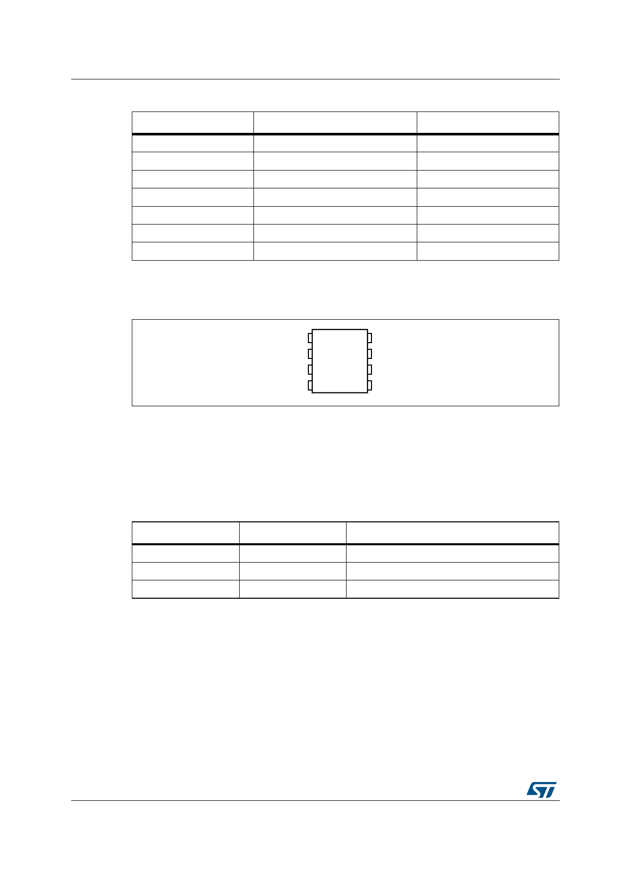
Figure 2. 8-pin package connections
5)GLVDEOH
$&
$&
966
9&&
*32
6&/
6'$
1. See Package mechanical data section for package dimensions, and how to identify pin 1.
069
1.1
1.1.1
1.1.2
Functional modes
The M24SR02-Y has two functional modes available. The difference between the modes
lies in the power supply source (see Table 2).
Modes
I2C mode
Tag mode
Dual interface mode
Table 2. Functional modes
Supply source
Comments
Vcc
RF field only
RF field or Vcc
The I2C interface is available
The I2C interface is disconnected
Both I2C and RF interfaces are available
I2C mode
M24SR02-Y is powered by VCC. The I2C interface is connected to the M24SR02-Y. The I2C
host can communicate with the M24SR02-Y device.
Tag mode
The M24SR02-Y is supplied by the RF field and can communicate with an RF host (RFID
reader or an NFC phone). The User memory can only be accessed by the RF commands.
10/90
DocID025386 Rev 10
Share Link: