SPX2810 데이터 시트보기 (PDF) - Signal Processing Technologies
부품명
상세내역
제조사
SPX2810 Datasheet PDF : 13 Pages
| |||
ABSOLUTE MAXIMUM RATINGS
Lead Temperature (soldering, 5 seconds) .................. 300°C
Storage Temperature Range ...................... -65°C to +150°C
Operating Junction Temperature Range ..... -40°C to +125°C
Input Supply Voltage ..................................................... +10V
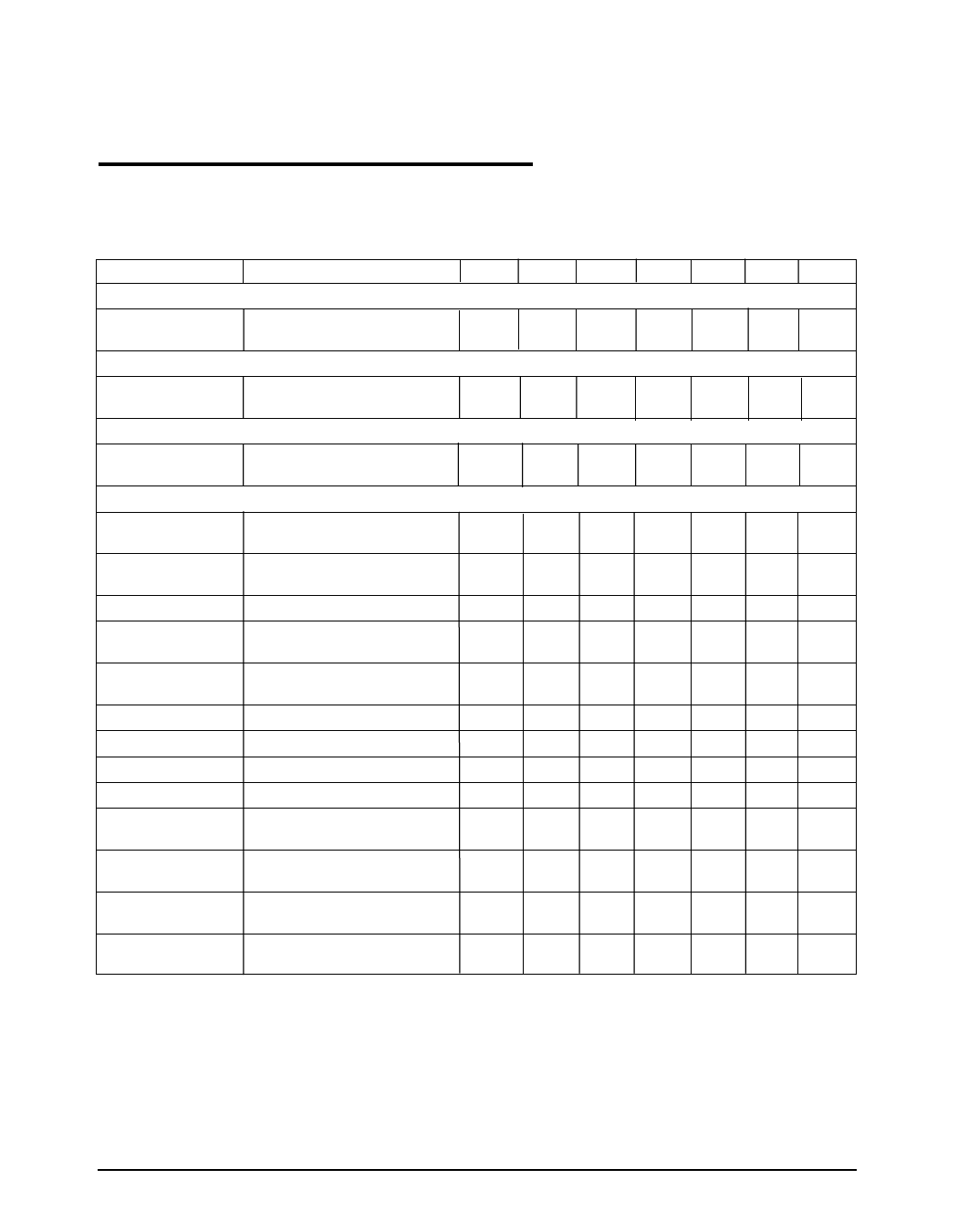
ELECTRICAL CHARACTERISITCS
VIN=VOUT + 1.5V, COUT = 10µF, at IOUT = 10mA, TA = 25°C, unless otherwise specified. Limits in Boldface applies
over the full operating temperature range.
PARAMETER
CONDITIONS
SPX2810A
MIN TYP MAX
SPX2810
MIN TYP MAX UNITS
2.5V Version
Output Voltage
(Note 2)
0
≤
I
OUT
=
1A,
4.0V
≤
V
IN
≤
10V
2.475 2.500 2.525 2.450 2.500 2.550
V
2.450
2.550 2.425
2.575
3.0V Version
Output Voltage
(Note 2)
0 ≤ IOUT = 1A, 4.5V ≤ VIN ≤ 10V
2.970 3.000 3.030 2.940 3.000 3.060
V
2.940
3.060 2.790
3.090
3.3V Version
Output Voltage
(Note 2)
0 ≤ IOUT = 1A, 4.8V ≤ VIN ≤ 10V
3.267 3.300 3.333 3.234 3.300 3.366
V
3.234
3.366 3.069
3.399
All Output Options
Reference Voltage
Min Load Current
(Note 3)
I =10mA, V = V +3V
OUT
IN OUT
10≤IOUT≤ 1A, 1.5V≤(VIN-VOUT)≤ 5.75V
1.5≤(VIN - VOUT)≤5.75V
1.238 1.250 1.263 1.225 1.250 1.275
V
1.225
1.281 1.212
1.288
5
10
10
mA
Line Regulation
Load Regulation
Dropout Voltage
(Note 2)
Current Limit
Long Term Stability
Thermal Regulation
RMS Output Noise
Thermal Resistance
2.75≤VIN≤ 7V, IOUT=TJ=25°C (Note 2)
0.005 0.2
(VIN - VOUT)=3.0V, 10mA≤IOUT≤ 1A,
TJ=25°C (Note 3)
0.05
0.3
IOUT=1A (Note 3)
IOUT=1A (Note 2)
1.1
1.2
1.05 1.15
VIN=7V,1.4≤(VIN-VOUT)(Note 3)
1.2
2.0
TA=25°C, 1000Hrs (Note2)
0.03
25°C, 20mS Pulse
0.01 0.02
TA=25°C, 10Hz≤f≤10kHz
TO-220 Junction to Tab
TO-220 Junction to Ambient
0.003
3.0
60
0.005 0.2
%
0.05
0.2
%
1.1
1.2
V
1.2
A
1.0
1.0
%
0.01 0.02 %/Ω
0.003
%
3.0 °C/W
60
TO-220 Junction to Tab
TO-220 Juinction to Ambient
3.0
3.0 °C/W
60
60
TO-220 Junction to Tab
TO-220 Junction to Ambient
6
6
°C/W
126
126 °C/W
SOT-223 Junction Tab
TO-220 Junction to Ambient
15
15
°CW
156
156 °C/W
NOTES:
Note 1: Output temperature coefficient is defined as the worst case voltage change divided by the total temperature range.
Note 2: Dropout voltage is defined as the input to output differential at which the output voltage drops 100mV below its nominal value measured at 1V differential at
very low values of programmed output voltage, the minimum input supply voltage of 2V ( 2.3V over temperature) must be taken into account.
Note 3: Thermal regulation is defined as the change in output voltage at a time T after a change in power dissipation is applied excluding load or line regulation effect.
Date: 5/25/04
SPX2810 1A Low Dropout Linear Regulator
2
© Copyright 2004 Sipex Corporation
Share Link: 