SPX2810 데이터 시트보기 (PDF) - Signal Processing Technologies
부품명
상세내역
제조사
SPX2810 Datasheet PDF : 13 Pages
| |||
(Note A)
V IN
+
4.7µF
SPX2810
5V
IN
OUT
V
OUT
ADJ
R1
1kΩ,
1%
*C 1 improves ripple rejection.
ZC should be ~ R1 at ripple frequency
R2
330Ω
1%
10µF
+ C1
10µF*
V IN
(Note A)
+
SPX2810
IN
OUT
ADJ
4.7µF
1k
TTL
Input
2N3904
1k
5V
1kΩ
1%
+
10µF
330Ω
1%
Note A: VIN(MIN) = (Intended VOUT ) + (V DROPOUT (MAX))
Note A: V = (Intended V ) + (V
)
IN(MIN)
OUT
DROPOUT (MAX)
Figure 10. Improving Ripple Rejection
Figure 11. 12.5V Regulator with Shutdown
Output Voltage
The output of the adjustable regulator can be set to any voltage between 1.25V and 10V. The value
of VOUT can be quickly approximated using the formula (Figure 9)
V =1.25 *(R1 + R2)/R1.
OUT
A small correction to this formula is required depending on the values of resistors R1 and R2, since
adjustable pin current (approx 50µA) flows through R2. When IADJ is taken into account, the formula
becomes
VOUT = VREF(1+ (R2/R1)) + IADJ * R2, where VREF=1.25V.
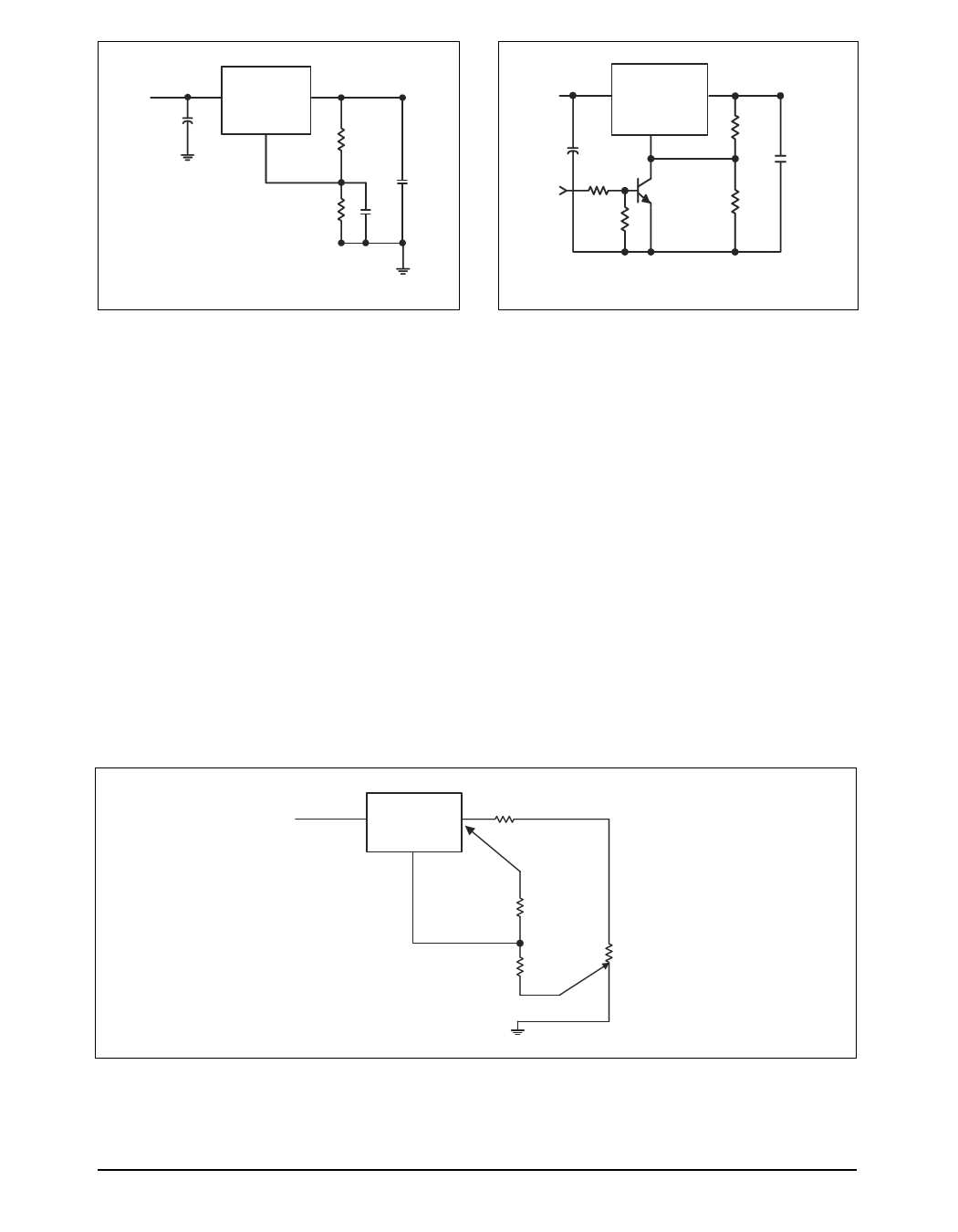
Layout Considerations
Parasitic line resistance can degrade load regulation. In order not to affect the behavior of the regulator,
it is best to connect R1 to the case as illustrated in Figure 11. For the same reason, R2 should be
connected to the negative side of the load.
RP Parasitic Line
Resistance
V IN
SPX2810
V OUT
Connect R1 to
Case of Regulator
ADJ
R1
RL
R2
Connect R2 to Load
Figure 12. Recommended Connections for Best Results
Date: 5/25/04
SPX2810 1A Low Dropout Linear Regulator
6
© Copyright 2004 Sipex Corporation
Share Link: 