MCM62449WJ35R2 데이터 시트보기 (PDF) - Motorola => Freescale
부품명
상세내역
제조사
MCM62449WJ35R2 Datasheet PDF : 7 Pages
| |||
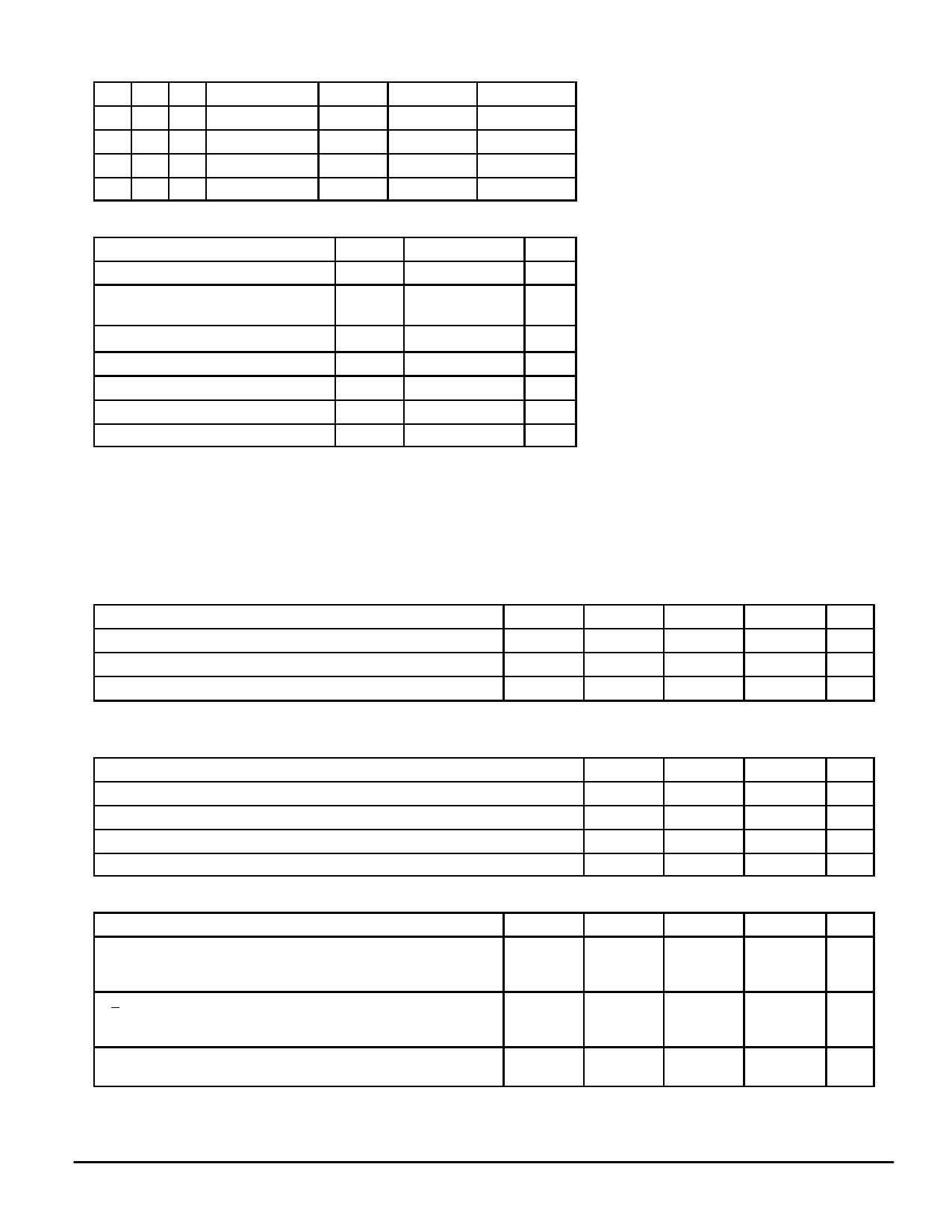
TRUTH TABLE (X = Don’t Care)
E GW
Mode
HXX
Not Selected
L H H Output Disabled
L LH
Read
LXL
Write
I/O Pin
High–Z
High–Z
Dout
High–Z
Cycle
—
—
Read
Write
Current
ISB1, ISB2
ICCA
ICCA
ICCA
ABSOLUTE MAXIMUM RATINGS (See Note)
Rating
Symbol
Value
Unit
Power Supply Voltage Relative to VSS
VCC
– 0.5 to + 7.0
V
Voltage Relative to VSS for Any Pin
Except VCC
Vin, Vout – 0.5 to VCC + 0.5 V
Output Current (per I/O)
Iout
± 20
mA
Power Dissipation
PD
1.0
W
Temperature Under Bias
Tbias
– 10 to + 85
°C
Operating Temperature
TA
0 to + 70
°C
Storage Temperature — Plastic
Tstg
– 55 to + 150
°C
NOTE: Permanent device damage may occur if ABSOLUTE MAXIMUM RATINGS are
exceeded. Functional operation should be restricted to RECOMMENDED OPER-
ATING CONDITIONS. Exposure to higher than recommended voltages for
extended periods of time could affect device reliability.
This device contains circuitry to protect the
inputs against damage due to high static
voltages or electric fields; however, it is ad-
vised that normal precautions be taken to avoid
application of any voltage higher than maxi-
mum rated voltages to these high impedance
circuits.
This CMOS memory circuit has been de-
signed to meet the dc and ac specifications
shown in the tables, after thermal equilibrium
has been established. The circuit is in a test
socket or mounted on a printed circuit board
and transverse air flow of at least 500 linear
feet per minute is maintained.
DC OPERATING CONDITIONS AND CHARACTERISTICS
(VCC = 5.0 V ± 10%, TA = 0 to + 70°C, Unless Otherwise Noted)
RECOMMENDED OPERATING CONDITIONS
Parameter
Supply Voltage (Operating Voltage Range)
Input High Voltage
Input Low Voltage
* VIL (min) = – 0.5 V dc; VIL (min) = – 2.0 V ac (pulse width ≤ 2.0 ns).
DC CHARACTERISTICS
Parameter
Input Leakage Current (All Inputs, Vin = 0 to VCC)
Output Leakage Current (E = VIH, Vout = 0 to VCC)
Output Low Voltage (IOL = + 8.0 mA)
Output High Voltage (IOH = – 4.0 mA)
Symbol
VCC
VIH
VIL
Min
4.5
2.2
– 0.5*
Symbol
Ilkg(I)
Ilkg(O)
VOL
VOH
Typ
Max
Unit
5.0
5.5
V
—
VCC + 0.3
V
—
0.8
V
Min
Max
Unit
—
± 1.0
µA
—
± 1.0
µA
—
0.4
V
2.4
—
V
POWER SUPPLY CURRENTS
Parameter
Symbol
Min
Typ
Max
Unit
AC Active Supply Current (Iout = 0 mA, MCM6249–20: tAVAV = 20 ns
ICC
—
175
190
mA
VCC = max)
MCM6249–25: tAVAV = 25 ns
—
160
175
MCM6249–35: tAVAV = 35 ns
—
145
160
AC Standby Current (VCC = max,
MCM6249–20: tAVAV = 20 ns
ISB1
—
50
60
mA
E = VIH, No other restrictions on
MCM6249–25: tAVAV = 25 ns
—
40
50
other inputs)
MCM6249–35: tAVAV = 35 ns
—
35
40
CMOS Standby Current (E ≥ VCC – 0.2 V, Vin ≤ VSS + 0.2 V or
≥ VCC – 0.2 V) (VCC = max, f = 0 MHz)
ISB2
—
10
15
mA
MCM6249
2
MOTOROLA FAST SRAM
Share Link: 