EL6252C 데이터 시트보기 (PDF) - Elantec -> Intersil
부품명
상세내역
제조사
EL6252C Datasheet PDF : 2 Pages
| |||
EL6252C - Product Brief
2-Channel laser diode Driver + Oscillator
Features
• Mini-Small Package Outline
• Voltage-controlled output current
source requiring one external set
resistor per channel
• Current-controlled output current
source.
• Rise time = 1.0 ns
• Fall time = 1.1 ns
• On chip oscillator with frequency
and amplitude control by use of
external resistors to ground
• Oscillator to 500 MHz
• Oscillator to 100 mA pk/pk
• Single +5V supply (±10%)
• Current amplification = 100
• CMOS control signals
Applications
• MO drives
• Mini-Disc drives
• Writable optical drives
• Laser diode current switching
Ordering Information
Part No
EL6252CY
Temp. Range
0°C to +70°C
Package
MSOP10
Outline #
MDP0043
General Description
The EL6252C is a high-performance two channel laser diode current
amplifier that provides controlled current to a grounded laser diode.
The write amplifier can provide over 200mA of DC or pulsed current.
The R and W channels have switching speeds of approximately one
nanosecond rise/fall time and are summed together at the IOUT output.
The level of the output current is set by an analog voltage applied to an
external resistor which converts the voltage into a current at the IIN pin
(virtually ground). The current seen at this pin is then amplified by
100X to become a current source at pin IOUT.
An on-chip 500 MHz oscillator is provided to allow current modula-
tion when in the read mode. This is turned on when the OSCEN pin is
held high (floating not recommended). Complete control of amplitude
and frequency is set by two external resistors connected to ground at
pins RFREQ and RAMP (see graphs in this data sheet for further
explanation).
Write current pulses appear when an ‘L’ signal is applied to the OUT-
ENW pin.
The external resistors allow the user to accurately and independently
set each amplifier transconductance by applying a voltage to each
resistor, without restriction on the voltage range, thus ensuring broad
voltage DAC compatibility. Alternatively, the IIN pin can be biased
from a current DAC or other current source.
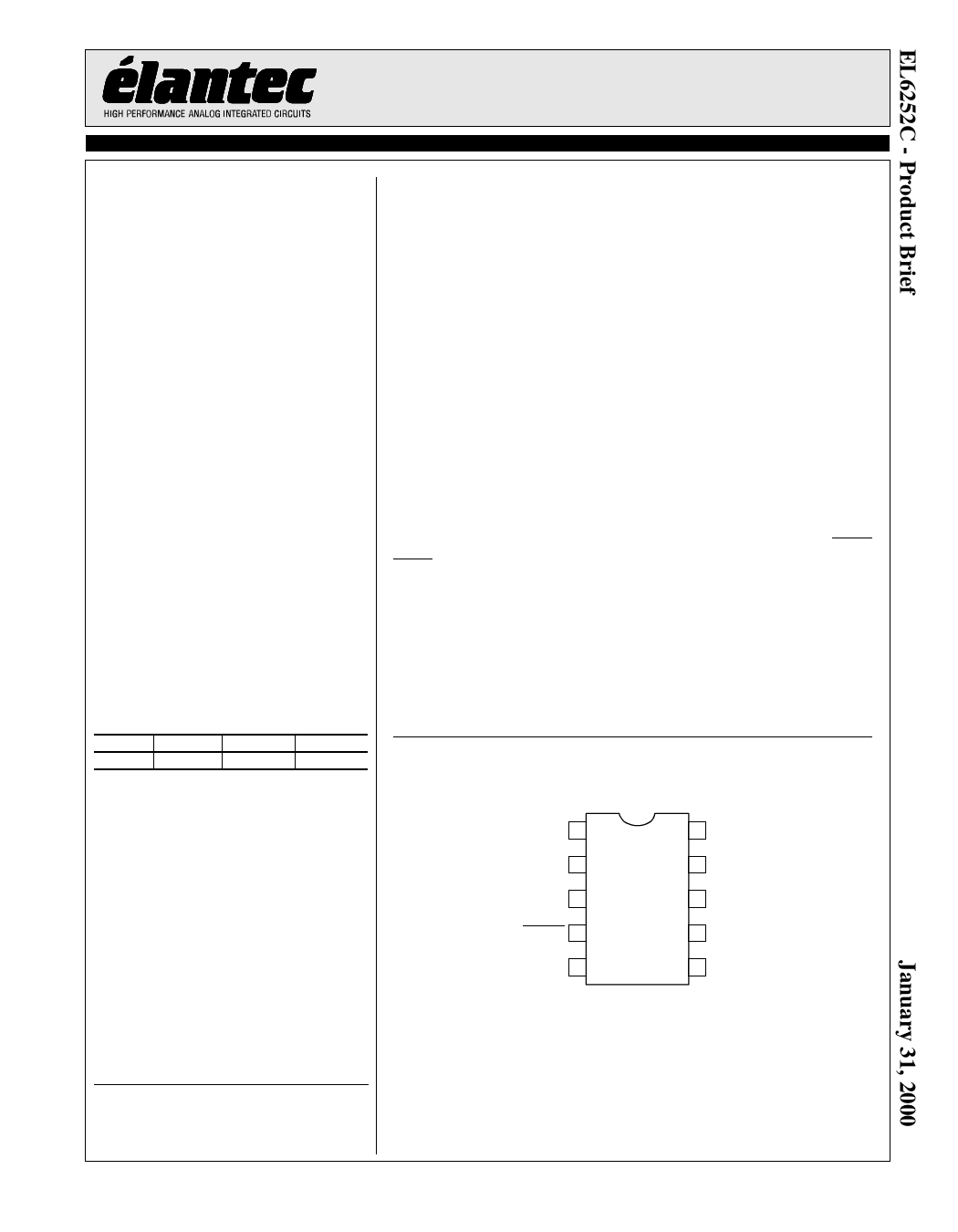
Connection Diagram
IINR 1
IINW 2
RFREQ 3
OUTENW 4
OSCEN 5
10 VCC
9 IOUT
8 GND
7 RAMP
6 VCC
Complete Product Specifications
Elantec Technical Support:
North America: 1-888-352-6832 X 311
Asia: +85-45-682-5820
Europe: +44-18-977-6020
©2000 Elantec Semiconductor, Inc.
Share Link: 