27C512 데이터 시트보기 (PDF) - Microchip Technology
부품명
상세내역
제조사
27C512 Datasheet PDF : 8 Pages
| |||
27C512A
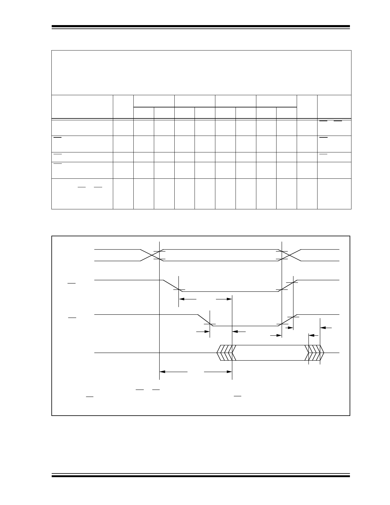
TABLE 1-3: READ OPERATION AC CHARACTERISTICS
AC Testing Waveform:
Output Load:
Input Rise and Fall Times:
Ambient Temperature:
VIH = 2.4V and VIL = .45V; VOH = 2.0V and VOL = 0.8V
1 TTL Load + 100 pF
10 ns
Commercial:
Tamb = 0˚C to +70˚C
Industrial:
Tamb = -40˚C to +85˚C
Extended (Automotive): Tamb = -40˚C to +125˚C
Parameter
Sym
27C512-90*
Min Max
27C512-10*
Min Max
27C512-12
Min Max
27C512-15
Units Conditions
Min Max
Address to Output
Delay
tACC —
90
— 100 — 120 — 150 ns CE = OE/
VPP = VIL
CE to Output Delay
tCE
—
90
— 100 — 120 — 150 ns OE/VPP =
VIL
OE to Output Delay
tOE
—
40
—
40
—
50
—
60
ns CE = VIL
OE to Output High
Impedance
tOFF
0
35
0
35
0
40
0
45 ns
Output Hold from
tOH
0
—
0
—
0
—
0
— ns
Address, CE or OE/
VPP, whichever
occurred first
*90/10 AC Testing Waveforms: VIH = 3.0V and VIL = 0V; VOH = 1.5V and VOL = 1.5V
Output Load: 1 TTL Load + 30 pF
FIGURE 1-1: READ WAVEFORMS
VIH
Address
VIL
VIH
CE
VIL
VIH
OE
VIL
Outputs VOH
O0 - O7 VOL
High Z
Address Valid
tCE(2)
tOE(2)
tACC
tOFF(1,3)
tOH
Valid Output
High Z
Notes: (1) tOFF is specified for OE or CE, whichever occurs first
(2) OE may be delayed up to t CE - t OE after the falling edge of CE without impact on tCE
(3) This parameter is sampled and is not 100% tested.
© 1996 Microchip Technology Inc.
DS11173E-page 3
Share Link: 