27C512 데이터 시트보기 (PDF) - Microchip Technology
부품명
상세내역
제조사
27C512 Datasheet PDF : 8 Pages
| |||
27C512A
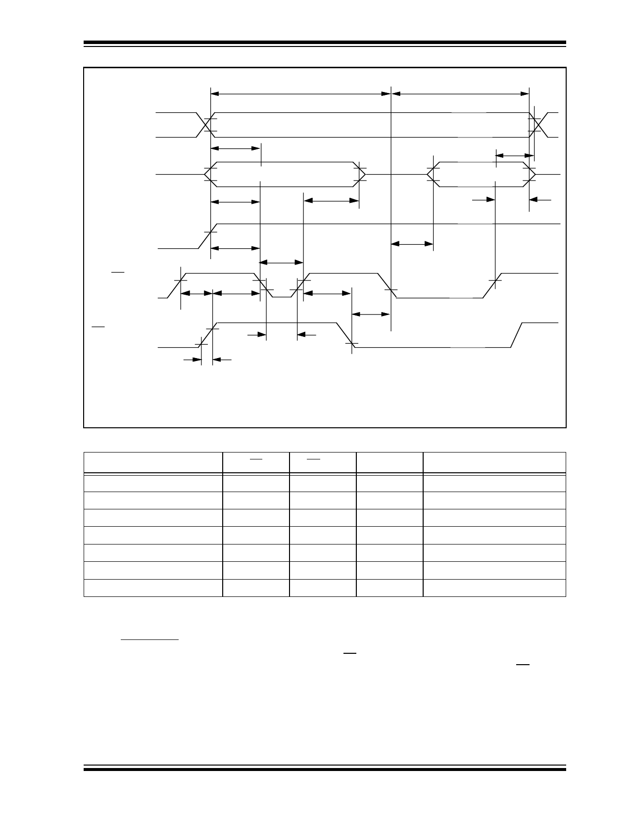
FIGURE 1-2: PROGRAMMING WAVEFORMS (1)
Program
Verify
VIH
Address VIL
VIH
Data VIL
Address Stable
tAS
Data In Stable
tDS
tDH
6.5 V (3)
VCC 5.0V
tCE
VIH
tVCS
tPW
(2)
CE VIL
tCES
tOES
tOEH
13.0 V (3)
OE/V PP
VIL
tPRT
tOR
tOPW
tAH
Data Out Valid
tDF
(2)
Notes: (1) The input timing reference level is 0.8V for VIL and 2.0V for VIH.
(2) tDF and tOE are characteristics of the device but must be accommodated by the programmer.
(3) VCC = 6.5V ±0.25V, V PP = VH = 13.0V ±0.5V for express programming algorithm.
TABLE 1-6: MODES
Operation Mode
Read
Program
Program Verify
Program Inhibit
Standby
Output Disable
Identity
X = Don’t Care
CE
OE/VPP
A9
VIL
VIL
X
VIL
VH
X
VIL
VIL
X
VIH
VH
X
VIH
X
X
VIL
VIH
X
VIL
VIL
VH
O0 - O7
DOUT
DIN
DOUT
High Z
High Z
High Z
Identity Code
1.2 Read Mode
(See Timing Diagrams and AC Characteristics)
Read Mode is accessed when
a) the CE pin is low to power up (enable) the chip
b) the OE/VPP pin is low to gate the data to the
output pins
For Read operations, if the addresses are stable, the
address access time (tACC) is equal to the delay from
CE to output (tCE). Data is transferred to the output
after a delay (tOE) from the falling edge of OE/VPP.
© 1996 Microchip Technology Inc.
DS11173E-page 5
Share Link: 