27C512 데이터 시트보기 (PDF) - Microchip Technology
부품명
상세내역
제조사
27C512 Datasheet PDF : 8 Pages
| |||
27C512A
1.3 Standby Mode
The standby mode is entered when the CE pin is high,
and the program mode is not identified.
When this conditions are met, the supply current will
drop from 25 mA to 30 µA.
1.4 Output Enable OE/VPP
This multifunction pin eliminates bus connection in mul-
tiple bus microprocessor systems and the outputs go to
high impedance when:
• the OE/VPP pin is high (VIH).
When a VH input is applied to this pin, it supplies the
programming voltage (VPP) to the device.
1.5 Erase Mode (UV Windowed Versions)
Windowed products offer the ability to erase the mem-
ory array. The memory matrix is erased to the all “1's”
state as a result of being exposed to ultraviolet light. To
ensure complete erasure, a dose of 15 watt-second/
cm2 is required. This means that the device window
must be placed within one inch and directly underneath
an ultraviolet lamp with a wavelength of 2537 Ang-
stroms, intensity of 12,000 mW/cm2 for approximately
40 minutes.
1.6 Programming Mode
The Express algorithm must be used for best results. It
has been developed to improve programming yields
and throughput times in a production environment. Up
to 10 100-microsecond pulses are applied until the byte
is verified. A flowchart of the Express algorithm is
shown in Figure 1-3.
Programming takes place when:
a) VCC is brought to the proper voltage,
b) OE/VPP is brought to the proper VH level, and
c) CE line is low.
Since the erased state is “1” in the array, programming
of “0” is required. The address to be programmed is set
via pins A0 - A15 and the data to be programmed is pre-
sented to pins O0 - O7. When data and address are
stable, a low going pulse on the CE line programs that
location.
1.7 Verify
After the array has been programmed it must be verified
to ensure all the bits have been correctly programmed.
This mode is entered when all the following conditions
are met:
a) VCC is at the proper level,
b) the OE/VPP pin is low, and
c) the CE line is low.
1.8 Inhibit
When programming multiple devices in parallel with dif-
ferent data, only CE needs to be under separate control
to each device. By pulsing the CE line low on a partic-
ular device, that device will be programmed; all other
devices with CE held high will not be programmed with
the data (although address and data will be available on
their input pins).
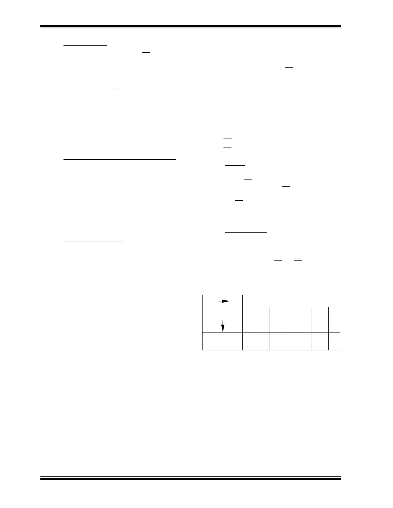
1.9 Identity Mode
In this mode specific data is output which identifies the
manufacturer as Microchip Technology Inc. and the
device type. This mode is entered when Pin A9 is taken
to VH (11.5V to 12.5V). The CE and OE/VPP lines must
be at VIL. A0 is used to access any of the two non-eras-
able bytes whose data appears on O0 through O7.
Pin
Input
Output
Identity
A0
0 OOOOOOO
76543210
H
e
x
Manufacturer VIL 0 0 1 0 1 0 0 1 29
Device Type* VIH 1 0 0 0 1 1 0 0 0D
* Code subject to change
DS11173E-page 6
© 1996 Microchip Technology Inc.
Share Link: 