HFA3925 데이터 시트보기 (PDF) - Intersil
부품명
상세내역
제조사
HFA3925 Datasheet PDF : 9 Pages
| |||
HFA3925
Pin Description (Continued)
PINS
SYMBOL
DESCRIPTION
17
18
19-22
VG3
VDD2
GND
Negative bias control for the third PA stage, adjusted to set VDD3 quiescent bias current, which is typically
90mA. Typical voltage at pin = -0.95V. Input impedance: > 1MΩ.
Positive bias for the second stage of the PA. 2.7V to 6V.
DC and RF Ground.
23
VDD3
Positive bias for the third stage of the PA. 2.7V to 6V.
24
GND
DC and RF Ground.
25
RF OUT
RF output of T/R switch and power amplifier for transmit mode.
26
T/R CTRL
0V for transmit mode, +5V for receive mode. Low < = 0.2V, high > = VDD -0.2V.
27
VDD TR
VDD for T/R switch.
28
GND
DC and RF Ground.
NOTE: Process variation will effect VG3 voltage requirement to develop 90mA stage 3 quiescent current, maximum range = -0.69V to -1.04V.
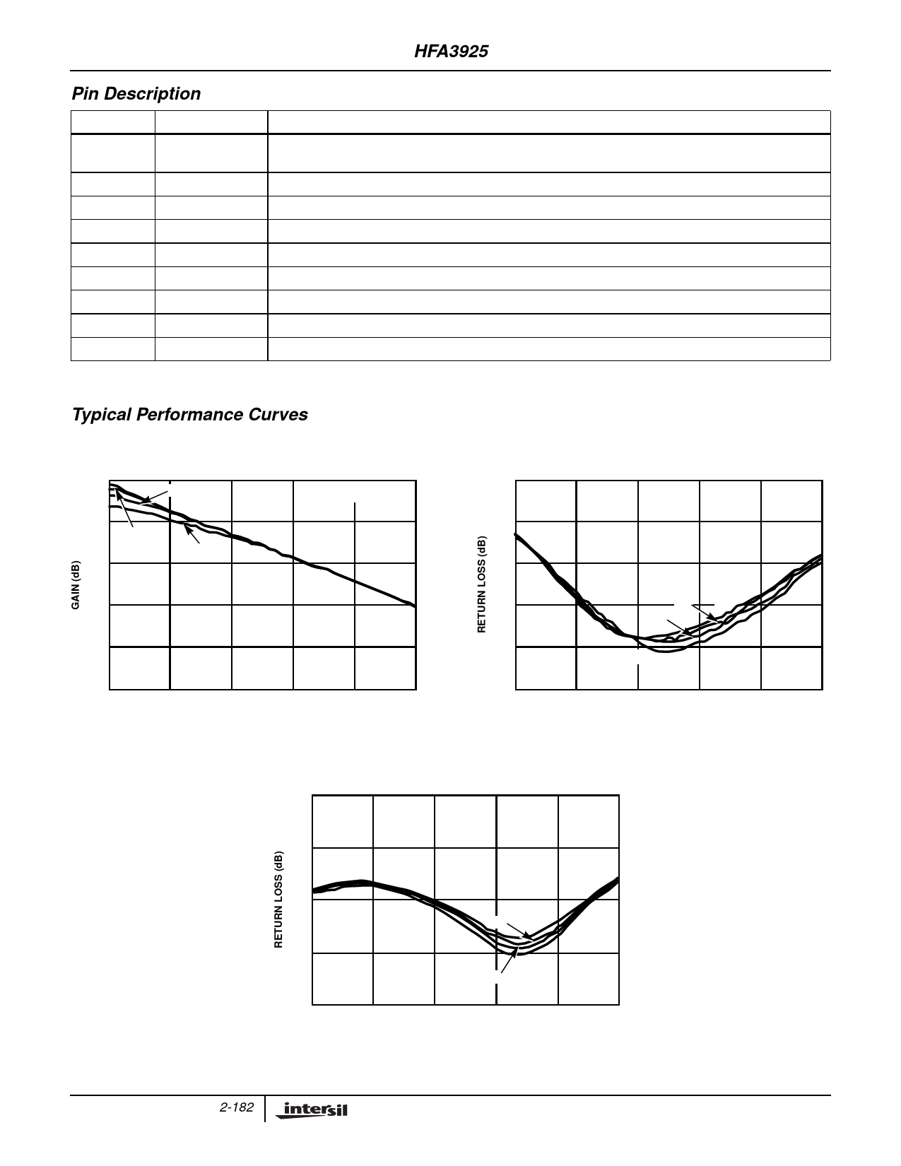
Typical Performance Curves
Power Amplifier Small Signal Performance NOTE: All data measured at TA = 25oC and VG1, VG2 and VG3 adjusted for first stage quies-
cent current of 20mA, second stage current of 53mA and third stage current of 90mA, respectively
35
6V 4V
-5
VDD1 = VDD2 = VDD3
30
-10
5V
3V
25
-15
20
15
10
2.0
2.2
2.4
2.6
2.8
3.0
FREQUENCY (GHz)
FIGURE 1. LINEAR GAIN
-20
5V
6V
4V
-25
3V
-30
2.0
2.2
2.4
2.6
2.8
3.0
FREQUENCY (GHz)
FIGURE 2. INPUT MATCH
0
-5
-10
5V
6V
3V
-15
4V
-20
2.0
2.2
2.4
2.6
2.8
3.0
FREQUENCY (GHz)
FIGURE 3. OUTPUT MATCH
2-182
Share Link: 