HFA3624 데이터 시트보기 (PDF) - Intersil
부품명
상세내역
제조사
HFA3624 Datasheet PDF : 19 Pages
| |||
HFA3624
Pin Descriptions (Continued)
PINS
23
24
26
27
28
2, 4, 6, 9, 11,
13, 18, 25
SYMBOL
RXM_IF-
RXM_IF+
RXM_RF
RX_VCC
RX_PE
GND
DESCRIPTION
Receive Channel Mixer IF- Output (10MHz to 400MHz). The RXM_IF+ and RXM_IF- pins form a compli-
mentary open collector output driver pair. The open collector outputs require an external load to VCC not to
exceed 500Ω, for the Single Ended IF case shown in Figure 3, or 1kΩ for the Differential IF cases shown in
Figures 2 and 4. This pin requires AC coupling.
Receive Channel Mixer IF+ Output (10MHz to 400MHz) The RXM_IF+ and RXM_IF- pins form a compli-
mentary open collector output driver pair. The open collector outputs require an external load to VCC not to
exceed 500Ω, for the Single Ended IF case shown in Figure 3, or 1kΩ for the Differential IF cases shown in
Figures 2 and 4. This pin requires AC coupling.
Receive Channel Mixer RF Input (2400MHz to 2500MHz). The nominal impedance of 50Ω, over the oper-
ating frequency range, is achieved with an on chip narrowband tuned circuit. This pin requires AC coupling.
Receive Channel Positive Power Supply. Use high quality decoupling capacitors right at the pin. A 200pF
chip capacitor is recommended.
Receive Channel Power Enable Control Input. TTL compatible input. Refer to “Power Control Truth Table”
on previous page.
Circuit Ground Pins (Qty 8). Internally connected.
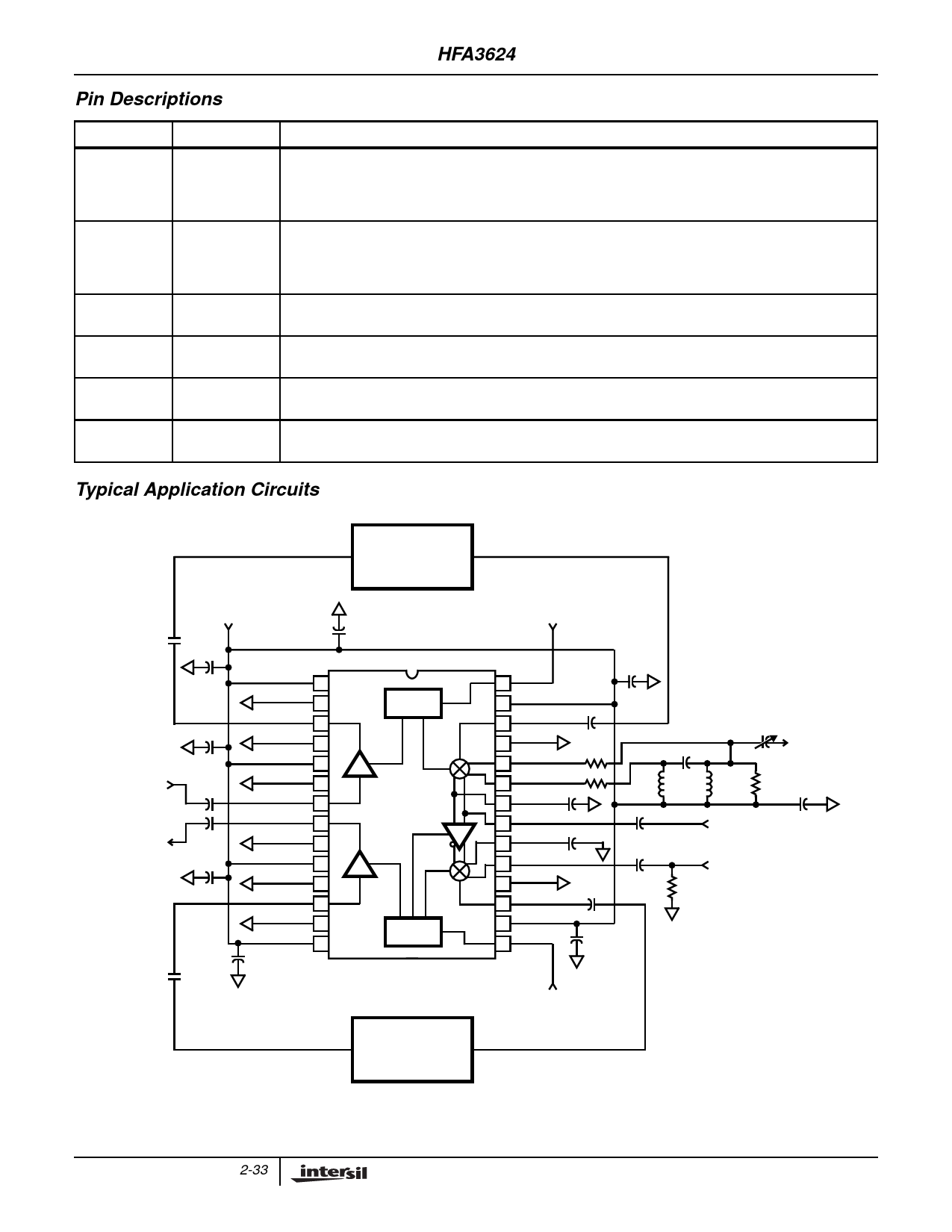
Typical Application Circuits
C14
RF INPUT
2450MHz
50Ω
RF OUTPUT
2450MHz
50Ω
C15
-3dB/50Ω BPF
2450MHz
LFJ30-03B2442B084
muRata
VCC = 2.7V
C12
C13
C41
C40
C11
RXA_VCC2 1
GND
2
RXA_OUT
3
GND
4
RXA_VCC1 5
GND
6
RXA_IN
7
TXA_OUT
8
GND
9
TXA_VCC2
10
GND
11
TXA_IN
12
GND
13
TXA_VCC1
14
C10
C32
RX BIAS
RXM
RXA
HFA3624
LOB
TXA
TXM
TX BIAS
-3dB/50Ω BPF
2450MHz
LFJ30-03B2442B084
muRata
RECEIVE
ENABLE
RX_PE
28
27 RX_VCC
RXM_RF
26
GND
25
C25
RXM_IF+ 22
24
RXM_IF- 22
23
LO_BY C27
22
LO_IN
21 TXM_IF- C28
20
19 TXM_IF+
GND
18
TXM_RF
C23
17
TX_VCC
16
TX_PE
15
C19
C21
L46
C26
C37
IF OUTPUT
280MHz
C51 250Ω
C45 L47
R50
LO INPUT
C48
2170MHz
50Ω
IF INPUT
R35 280MHz, 250Ω
250Ω
TRANSMIT
ENABLE
FIGURE 2. DIFFERENTIAL TO SINGLE ENDED IF OUTPUT TRANSLATION WITH 250Ω IF IMPEDANCE
2-33
Share Link: 