L6260 데이터 시트보기 (PDF) - STMicroelectronics
부품명
상세내역
제조사
L6260 Datasheet PDF : 30 Pages
| |||
L6260
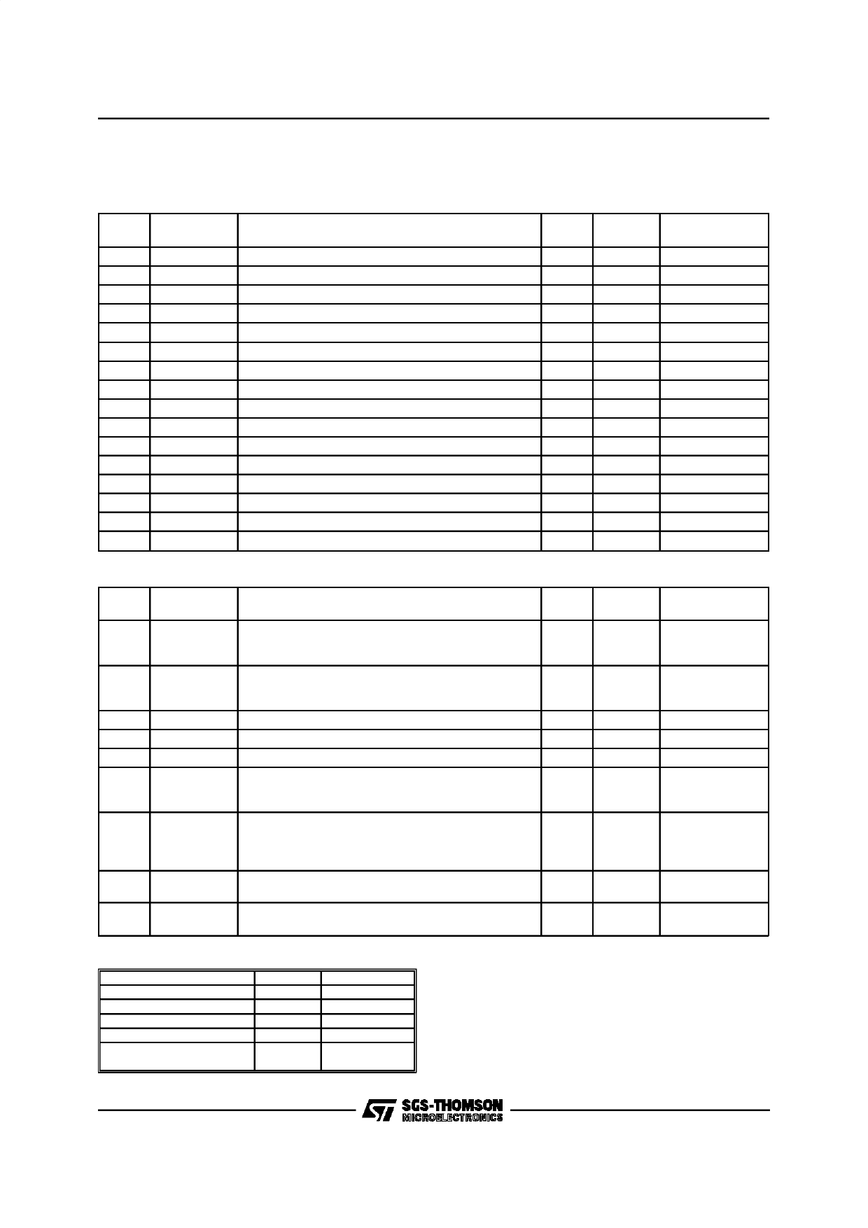
PIN DESCRIPTION
Pin Types: I = Input, O = Output, P = Power, A = Analog (passive)
Power
PIN # PIN NAME
DESCRIPTION
8
41
54
58
23
31
1
15-17
32-34
47-49
18
27
44
45
7
63
VDC
VCC
VVCM_1
VVCM_2
VSPIN_1
VSPIN_2
GND
GND
GND
GND
SPN_GND_1
SPN_GND_2
DAC_GND
AGND
DIG_GND
TRIPGND
Digital power. Positive nominally 5V or 3V
Analog power. Positive nominally 5V or 3V
VCM power supply. Positive nominally 5V or 3V
Same as above
Spindle power pin. Positive nominally 5V or 3V
Same as above
Ground
Ground
Ground
Ground
Ground for spindle circuit
As above
Ground for all DACs
Analog ground
Digital ground
Voltage tripler ground
PIN
I\O
TRI-STATE
TYPE MAPPED? @SLEEP/@POR
AI
No
No
AI
No
No
AI
No
No
AI
No
No
AI
No
No
AI
No
No
AI
No
No
AI
No
No
AI
No
No
AI
No
No
AI
No
No
AI
No
No
AI
No
No
AI
No
No
AI
No
No
AI
No
No
Serial Interface & Test Pins
PIN #
12
11
10
19
9
21
24
60
26
PIN NAME
FCLCK
SDIO
SCLK
R/W
SLOAD
TEST
TRISTATE
ATEST
DTEST
DESCRIPTION
System clock. 4-12MHz selectable via the
CLK_PRESCALE bit in the System Control Register
B (Reg 4 Bit 4).
Serial port data I/O running up to 10MHz. For full
details of all serial port signals see the Circuit
Description section.
Serial port clock (max 10Mbits/s)
Read / Write signal for serial interface
Chip select input.
Used to enable one of the test modes. The mode is
selcted in conjunction with the TRISTATE pin (see
below for more details).
Used to enable one of the test modes. The mode is
selcted in conjunction with the TEST pin (see below
for more details). This pin has no effect on the
spindle or VCM drivers, this is a test pin only.
Analog test pin. This pin carries the required analog
signal to allow external testing.
Digital Test Output Pin. This pin also doubles as the
Clock input if an external FLL is used.
PIN
I\O
TRI-STATE
TYPE MAPPED? @SLEEP/@POR
DI
Yes
No
DI/O
Yes
Yes
DI
Yes
No
DI
Yes
No
DI
Yes
No
DI
No
No
DI
No
No
AO
No
No
DI/O
No
No
Test Mode
IOMAPPING Test
DIGITAL Test*
ANALOG Test*
TRISTATE Test
Normal Operation (non
test mode)
TEST pin
1
1
1
0
0
TRISTATE pin
0
1
1
1
0
For a detailed description please refer to the Test
Circuit section of the CIRCUIT OPERATION por-
tion of this datasheet
* These two test modes operate simultaneously through separate
test pins (ATEST and DTEST).
3/30
Share Link: 