L6260 데이터 시트보기 (PDF) - STMicroelectronics
부품명
상세내역
제조사
L6260 Datasheet PDF : 30 Pages
| |||
L6260
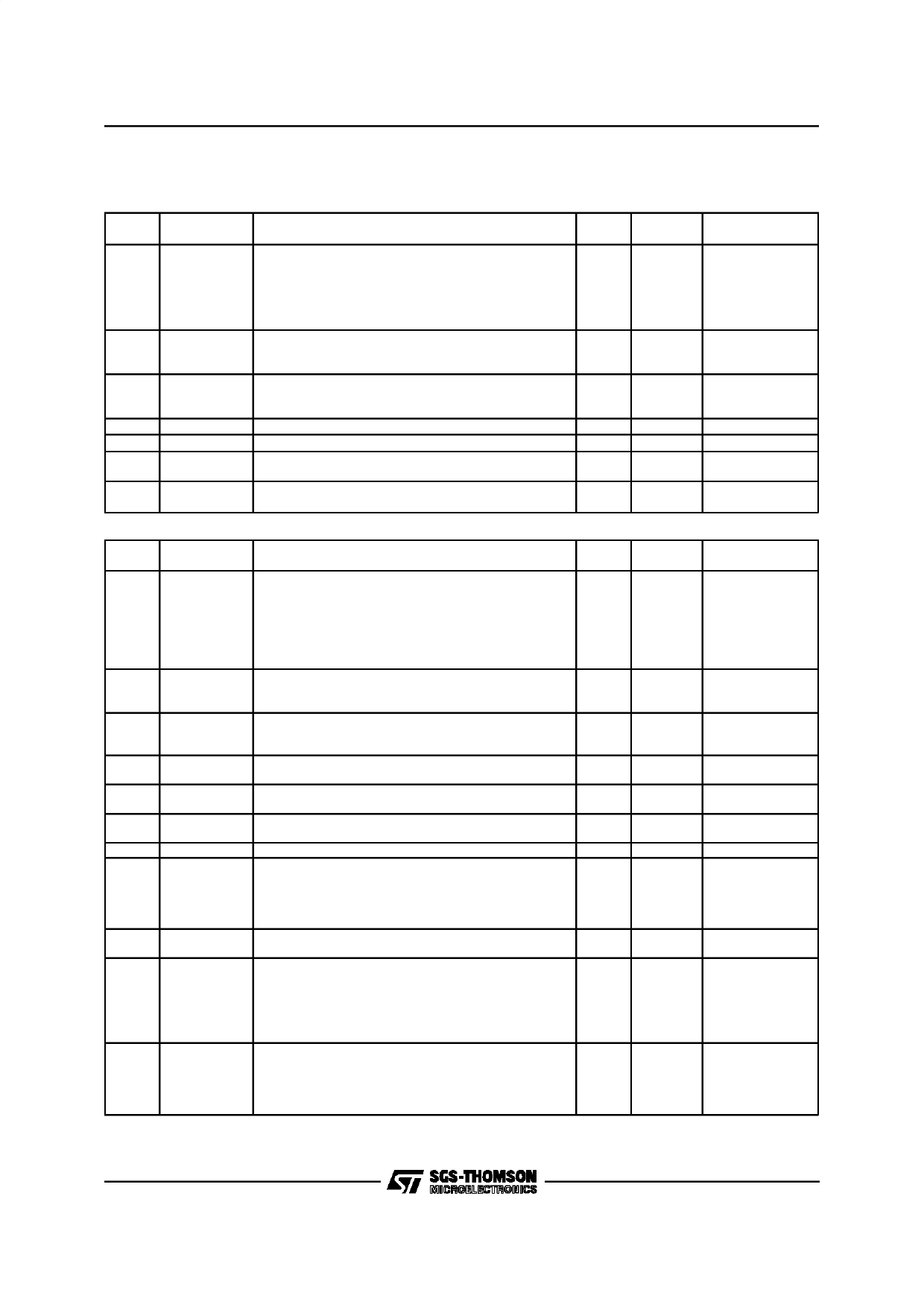
PIN DESCRIPTION (continued)
Pin Types: I = Input, O = Output, P = Power, A = Analog (passive)
VCM Driver and DAC
PIN # PIN NAME
DESCRIPTION
53 VCM_I_SNS1 High side of VCM sense resistor network. This pin
provides the current to the network as well as
sensing the total voltage across both sense
resistors. Sensing the total drop across both
resistors results in the low transconductance gain
feedback used for track following.
56 VCM_I_SNS2 Sensing across the lower VCM sense resistor for
high transconductance gain feedback for seek
operations.
6 VCM_COMP VCM compensation network. Typically, 200KΩ in
series with 100nF is connected from this pin to
Ground.
57 VCM_PLUS VCM Power Amplifier positive output terminal
55 VCM_MINUS VCM Power Amplifier negative output terminal
46
PARK_V A resistor conneced between this pin and
VCM_PLUS determines the Parking Voltage
35 VPARKOUT Output from the retract circuit. This pin is usually
directly connected to the VCM_MINUS.
Spindle Driver and DAC
PIN # PIN NAME
DESCRIPTION
40 SPN_SLEW The External.Spindle Driver Slew Rate resistor
(Rslew), typically 250K is connected from this pin to
Ground. When in nExternal Slew Rate Mode
(System Control Register B, Bit 10=0), the slew rate
is determined by:
Slew Rate = (0.5V to Rslew) X (DAC slew +1) +20pF
DAC slew = System Control Register bits 7 - 9.
36 SPN_I_COMP A seroies RC network from this pin to ground sets
the spin driver compensation. Typical a single 4nF
capacitor will provide adequate compensation.
14 SPN_I_SNS A current sensing resistor (2.5KΩ Typical ).is
connected from this pin to ground. See the Circuit
Operation section for details.
20
COIL_A Spindle Power Amplifier output A. Also serves as
BEMF sensing for Phase A.
25
COIL_B Spindle Power Amplifier output B. Also serves as
BEMF sensing for Phase B.
29
COIL_C Spindle Power Amplifier output C. Also serves as
BEMF sensing for Phase C.
59
CTAP
Spindle Motor Center Tap connection
22 SYNTH_HALL CMOS level spindle speed output. When SYNHALL
(System Control Register B, bit 5) is set to 0, this
output switches state at every zero crossing of any
phase. With SYNHALL = 1, the output only switches
every zero crossing of Phase A.
37 SPD_COMP Change Pump RC network connection pin for FLL
mode operation.
38 SPD_COMP_S This pin allows for shorting of to the Charge Pump
HT
Network resistor. This operation provides a quick
charge on the Charge Pump capacitor, reducing
settling time once desired speed is reached.
Operation is controlled by bit 9 of System Control
Register A.
39
FLL_RES Frequency Locked Loop charge pump gain resistor.
(Rep), typically 12.5KΩ , is connected from this pin
to Ground. Change Pump current is determined by:
I = (0.5V to Rcp) X (FLLGAIN DAC +1)
FLLGAIN DAC = System Control Register B bits 0-4
PIN
I\O
TRI-STATE
TYPE MAPPED? @SLEEP/@POR
A
No
No
A
No
No
A
No
No
A
No
No
A
No
No
A
No
No
AO
No
No
PIN
I\O
TRI-STATE
TYPE MAPPED? @SLEEP/@POR
A
No
No
A
No
No
AO
No
No
A
No
No
A
No
No
A
No
No
A
No
No
DO
Yes
Yes
A
No
No
A
No
No
A
No
No
4/30
Share Link: 