MT28C3212P2FL 데이터 시트보기 (PDF) - Micron Technology
부품명
상세내역
제조사
MT28C3212P2FL Datasheet PDF : 47 Pages
| |||
2 MEG x 16 PAGE FLASH
128K x 16 SRAM COMBO MEMORY
BALL DESCRIPTIONS
66-BALL FBGA
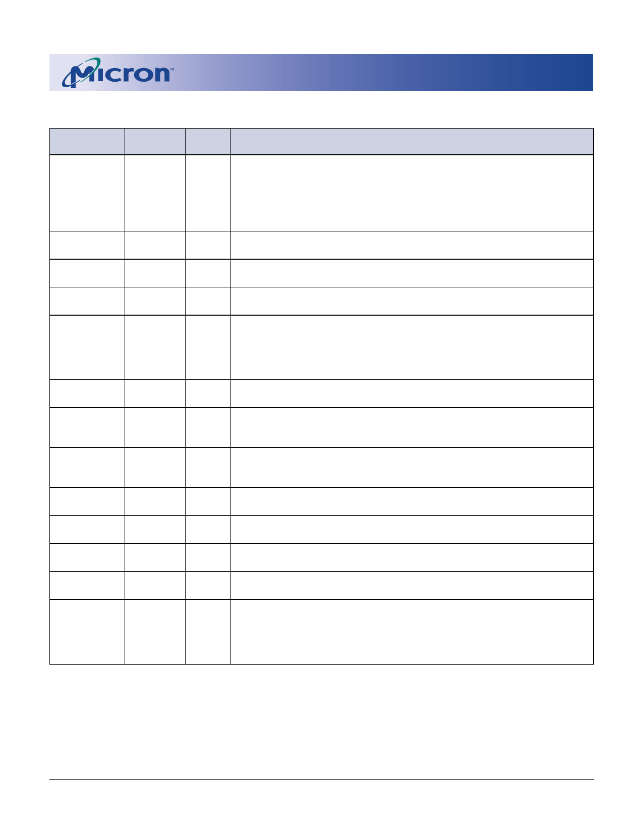
NUMBERS
A3, A4, A5, A6,
A7, A8, B3, B4,
B5, B6, E5, G3,
G4, G5, G6, G7,
G8, G9, H4, H5,
H6
H7
SYMBOL
A0–A20
F_CE#
TYPE
Input
Input
H9
F_OE# Input
C3
F_WE# Input
D4
F_RP# Input
E3
F_WP# Input
G10
S_CE1# Input
D8
S_CE2 Input
F5
S_OE# Input
B8
S_WE# Input
F3
S_LB# Input
F4
S_UB# Input
B7, B9, B10, DQ0–DQ15 Input/
C7, C8, C9,
Output
C10, D7, E6,
E8, E9, E10,
F7, F8, F9, F10
DESCRIPTION
Address Inputs: Inputs for the addresses during READ and WRITE
operations. Addresses are internally latched during READ and WRITE
cycles. Flash: A0–A20; SRAM: A0–A16.
Flash Chip Enable: Activates the device when LOW. When CE# is HIGH,
the device is disabled and goes into standby power mode.
Flash Output Enable: Enables Flash output buffers when LOW. When
F_OE# is HIGH, the output buffers are disabled.
Flash Write Enable: Determines if a given cycle is a Flash WRITE cycle.
F_WE# is active LOW.
Reset. When F_RP# is a logic LOW, the device is in reset, which drives
the outputs to High-Z and resets the WSM. When F_RP# is a logic HIGH,
the device is in standard operation. When F_RP# transitions from logic
LOW to logic HIGH, the device resets all blocks to locked and defaults to
the read array mode.
Flash Write Protect. Controls the lock down function of the flexible
locking feature.
SRAM Chip Enable1: Activates the SRAM when it is LOW. HIGH level
deselects the SRAM and reduces the power consumption to standby
levels.
SRAM Chip Enable2: Activates the SRAM when it is HIGH. LOW level
deselects the SRAM and reduces the power consumption to standby
levels.
SRAM Output Enable: Enables SRAM output buffers when LOW. When
S_OE# is HIGH, the output buffers are disabled.
SRAM Write Enable: Determines if a given cycle is an SRAM WRITE cycle.
S_WE# is active LOW.
SRAM Lower Byte: When LOW, it selects the SRAM address lower byte
(DQ0–DQ7).
SRAM Upper Byte: When LOW, it selects the SRAM address upper byte
(DQ8–DQ15).
Data Inputs/Outputs: Input array data on the second CE# and WE#
cycle during PROGRAM command. Input commands to the command
user interface when CE# and WE# are active. Output data when CE#
and OE# are active.
(continued on next page)
2 Meg x 16 Page Flash 128K x 16 SRAM Combo Memory
MT28C3212P2FL_2.p65 – Rev. 2, Pub. 4/02
5
Micron Technology, Inc., reserves the right to change products or specifications without notice.
©2002, Micron Technology, Inc.
Share Link: 