2SJ278MYTR-E 데이터 시트보기 (PDF) - Renesas Electronics
부품명
상세내역
제조사
2SJ278MYTR-E Datasheet PDF : 9 Pages
| |||
2SJ278
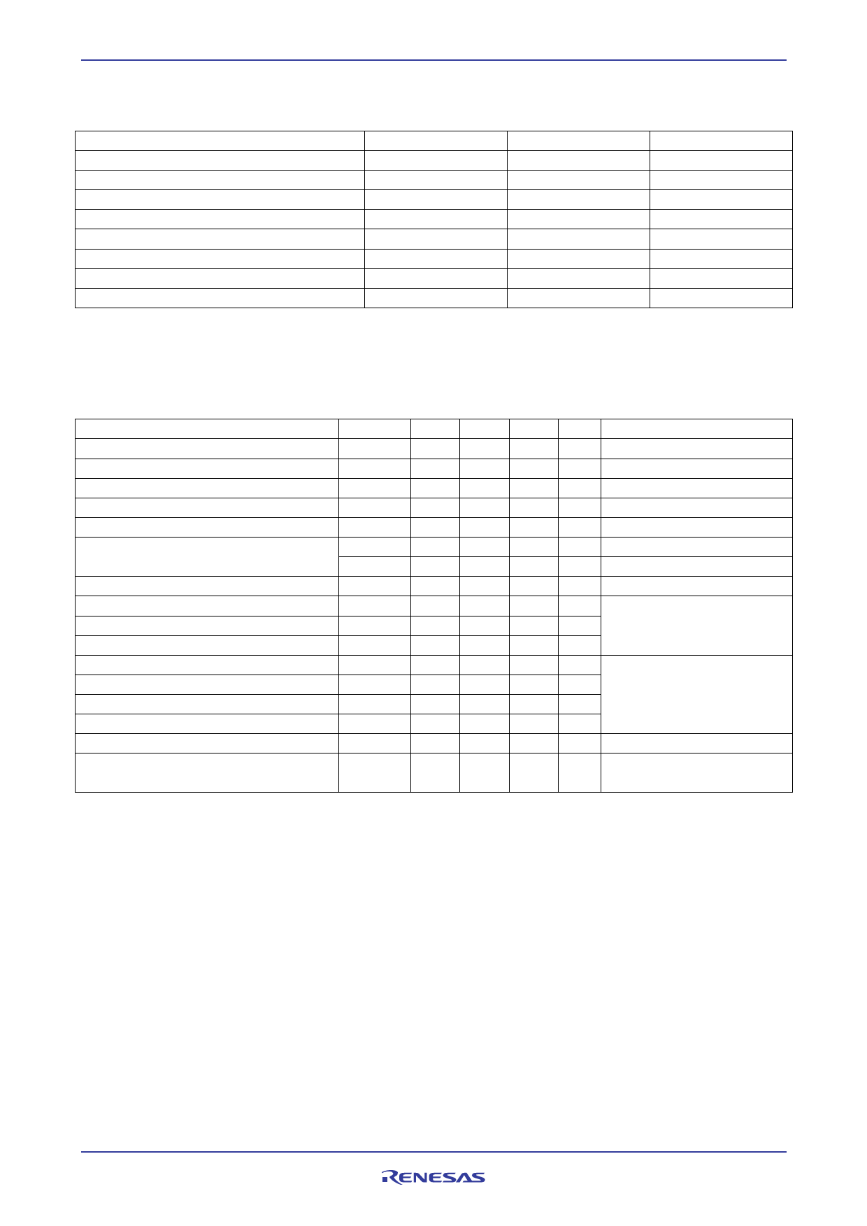
Absolute Maximum Ratings
Item
Symbol
Drain to source voltage
VDSS
Gate to source voltage
VGSS
Drain current
Drain peak current
ID
ID (pulse) Note 1
Body to drain diode reverse drain current
Channel dissipation
IDR
Pch Note 2
Channel temperature
Tch
Storage temperature
Tstg
Notes: 1. PW ≤ 10 µs, duty cycle ≤ 1%
2. Value on the alumina ceramic board (12.5 × 20 × 0.7 mm)
Value
–60
±20
–1
–4
–1
1
150
–55 to +150
(Ta = 25°C)
Unit
V
V
A
A
A
W
°C
°C
Electrical Characteristics
Item
Drain to source breakdown voltage
Gate to source breakdown voltage
Gate to source leak current
Zero gate voltage drain current
Gate to source cutoff voltage
Static drain to source on state resistance
Forward transfer admittance
Input capacitance
Output capacitance
Reverse transfer capacitance
Turn-on delay time
Rise time
Turn-off delay time
Fall time
Body to drain diode forward voltage
Body to drain diode reverse recovery time
Note: 3. Pulse test
Symbol
V (BR) DSS
V (BR) GSS
IGSS
IDSS
VGS (off)
RDS (on)
RDS (on)
|yfs|
Ciss
Coss
Crss
td (on)
tr
td (off)
tf
VDF
trr
Min
–60
±20
—
—
–1.0
—
—
0.6
—
—
—
—
—
—
—
—
—
Typ
—
—
—
—
—
0.7
0.9
1.0
160
80
28
7
8
30
25
–1.1
90
Max
—
—
±5
–10
–2.25
0.83
1.2
—
—
—
—
—
—
—
—
—
—
Unit
V
V
µA
µA
V
Ω
Ω
S
pF
pF
pF
ns
ns
ns
ns
V
ns
(Ta = 25°C)
Test Conditions
ID = –10 mA, VGS = 0
IG = ±100 µA, VDS = 0
VGS = ±16 V, VDS = 0
VDS = –50 V, VGS = 0
ID = –1 mA, VDS = –10 V
ID = –0.5 A, VGS = –10 V Note 3
ID = –0.5 A, VGS = –4 V Note 3
ID = –0.5 A, VDS = –10 V Note 3
VDS = –10 V
VGS = 0
f = 1 MHz
ID = –0.5 A
VGS = –10 V
RL = 60 Ω
IF = –1 A, VGS = 0
IF = –1 A, VGS = 0
diF/dt = 50 A/µs
Rev.2.00 Sep 07, 2005 page 2 of 6
Share Link: 