2SK3815 데이터 시트보기 (PDF) - SANYO -> Panasonic
부품명
상세내역
제조사
2SK3815 Datasheet PDF : 5 Pages
| |||
2SK3815
Electrical Characteristics at Ta=25°C
Parameter
Drain-to-Source Breakdown Voltage
Zero-Gate Voltage Drain Current
Gate-to-Source Leakage Current
Cutoff Voltage
Forward Transfer Admittance
Static Drain-to-Source On-State Resistance
Input Capacitance
Output Capacitance
Reverse Transfer Capacitance
Turn-ON Delay Time
Rise Time
Turn-OFF Delay Time
Fall Time
Total Gate Charge
Gate-to-Source Charge
Gate-to-Drain “Miller” Charge
Diode Forward Voltage
Symbol
Conditions
V(BR)DSS
IDSS
IGSS
VGS(off)
⏐yfs⏐
RDS(on)1
RDS(on)2
Ciss
Coss
Crss
td(on)
tr
td(off)
tf
Qg
Qgs
Qgd
VSD
ID=1mA, VGS=0V
VDS=60V, VGS=0V
VGS= ±16V, VDS=0V
VDS=10V, ID=1mA
VDS=10V, ID=12A
ID=12A, VGS=10V
ID=12A, VGS=4V
VDS=20V, f=1MHz
VDS=20V, f=1MHz
VDS=20V, f=1MHz
See specified Test Circuit.
See specified Test Circuit.
See specified Test Circuit.
See specified Test Circuit.
VDS=30V, VGS=10V, ID=23A
VDS=30V, VGS=10V, ID=23A
VDS=30V, VGS=10V, ID=23A
IS=23A, VGS=0V
Ratings
Unit
min
typ
max
60
V
1 µA
±10 µA
1.2
2.6
V
9
15
S
42
55 mΩ
60
85 mΩ
775
pF
125
pF
105
pF
11
ns
85
ns
72
ns
78
ns
19
nC
2.5
nC
4.1
nC
1.04
1.5
V
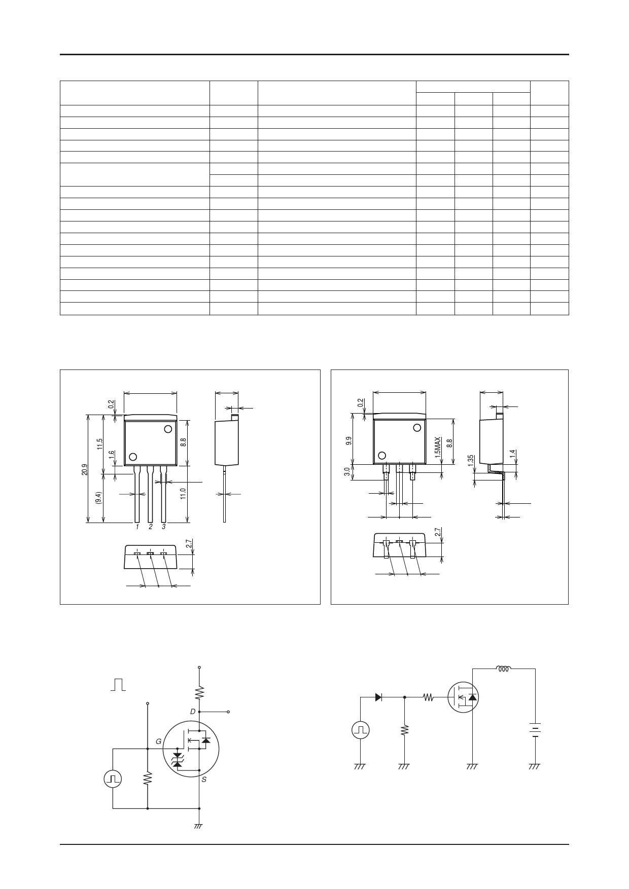
Package Dimensions
unit : mm (typ)
7513-002
Package Dimensions
unit : mm (typ)
7001-003
10.2
4.5
1.3
10.2
4.5
1.3
1.2
0.8
0.4
123
2.55
2.55
1 : Gate
2 : Drain
3 : Source
SANYO : SMP
12
0.8
2.55
3
1.2
2.55
2.55
2.55
0 to 0.3
0.4
1 : Gate
2 : Drain
3 : Source
SANYO : SMP-FD
Switching Time Test Circuit
VIN
10V
0V
VIN
PW=10µs
D.C.≤1%
G
VDD=30V
ID=12A
RL=2.5Ω
D
VOUT
2SK3815
P.G
50Ω
S
Unclamped Inductive Test Circuit
≥50Ω
RG
L
DUT
15V
0V
50Ω
VDD
No.8053-2/5
Share Link: 