M29W102BT90N6T 데이터 시트보기 (PDF) - STMicroelectronics
부품명
상세내역
제조사
M29W102BT90N6T
STMicroelectronics

M29W102BT90N6T Datasheet PDF : 20 Pages
| |||
M29W102BT, M29W102BB
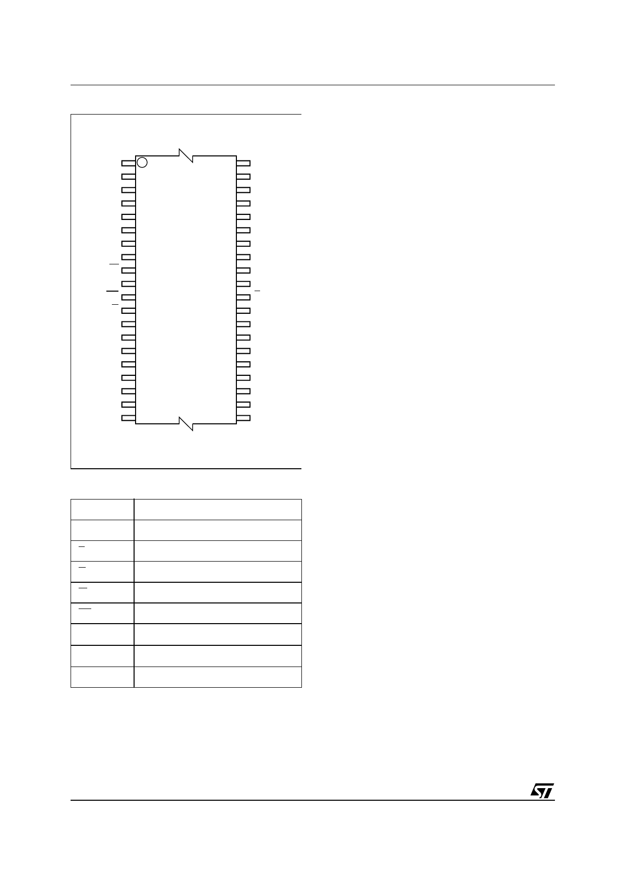
Figure 2. TSOP Connections
A9
A10
A11
A12
A13
A14
A15
NC
W
VCC
RP
E
DQ15
DQ14
DQ13
DQ12
DQ11
DQ10
DQ9
DQ8
1
40
10 M29W102BT 31
11 M29W102BB 30
20
21
AI02786
VSS
A8
A7
A6
A5
A4
A3
A2
A1
A0
G
DQ0
DQ1
DQ2
DQ3
DQ4
DQ5
DQ6
DQ7
VSS
Table 1. Signal Names
A0-A15
Address Inputs
DQ0-DQ15 Data Inputs/Outputs
E
Chip Enable
G
Output Enable
W
Write Enable
RP
Reset/Block Temporary Unprotect
VCC
Supply Voltage
VSS
Ground
NC
Not Connected Internally
SUMMARY DESCRIPTION
The M29W102B is a 1 Mbit (64Kb x16) non-vola-
tile memory that can be read, erased and repro-
grammed. These operations can be performed
using a single low voltage (2.7 to 3.6V) supply. On
power-up the memory defaults to its Read mode
where it can be read in the same way as a ROM or
EPROM.
The memory is divided into blocks that can be
erased independently so it is possible to preserve
valid data while old data is erased. Each block can
be protected independently to prevent accidental
Program or Erase commands from modifying the
memory. Program and Erase commands are writ-
ten to the Command Interface of the memory. An
on-chip Program/Erase Controller simplifies the
process of programming or erasing the memory by
taking care of all of the special operations that are
required to update the memory contents. The end
of a program or erase operation can be detected
and any error conditions identified. The command
set required to control the memory is consistent
with JEDEC standards.
The blocks in the memory are asymmetrically ar-
ranged, see Tables 3 and 4, Block Addresses. The
first or last 32 Kwords have been divided into four
additional blocks. The 8 Kword Boot Block can be
used for small initialization code to start the micro-
processor, the two 4 Kword Parameter Blocks can
be used for parameter storage and the remaining
16 Kwords are a small Main Block where the appli-
cation may be stored.
Chip Enable, Output Enable and Write Enable sig-
nals control the bus operation of the memory.
They allow simple connection to most micropro-
cessors, often without additional logic.
The memory is offered in a TSOP40 (10 x 14mm)
package and it is supplied with all the bits erased
(set to ’1’).
2/20
Share Link: