MAX4066 데이터 시트보기 (PDF) - Maxim Integrated
부품명
상세내역
제조사
MAX4066 Datasheet PDF : 12 Pages
| |||
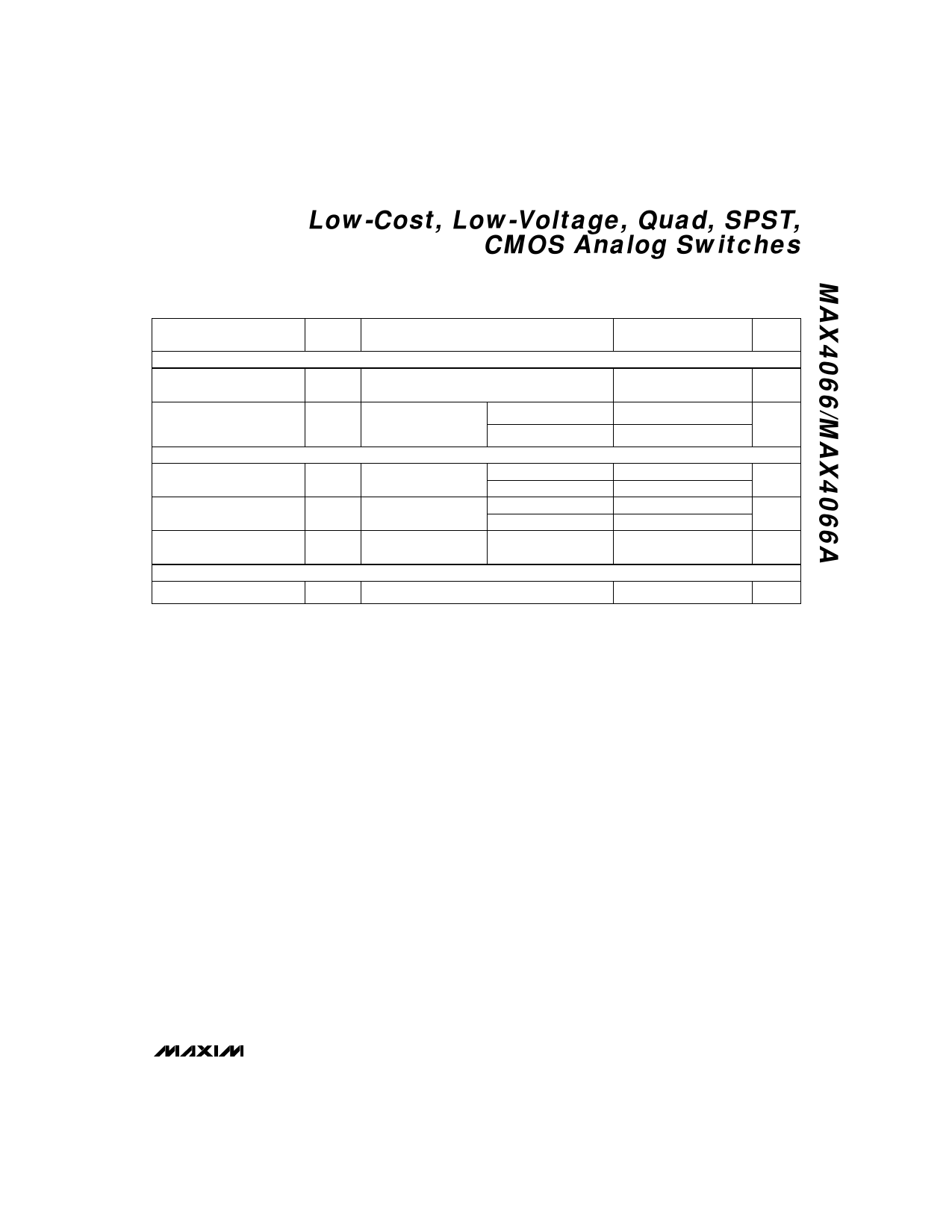
Low-Cost, Low-Voltage, Quad, SPST,
CMOS Analog Switches
ELECTRICAL CHARACTERISTICS—Single +3V Supply
(V+ = 2.7V to 3.3V ±10%, GND = 0V, VINH = 2.4V, VINL = 0.8V, TA = TMIN to TMAX, unless otherwise noted.)
PARAMETER
ANALOG SWITCH
Analog Signal Range
Channel On-Resistance
DYNAMIC
Turn-On Time (Note 3)
Turn-Off Time (Note 3)
Charge Injection (Note 3)
SUPPLY
Positive Supply Current
SYMBOL
CONDITIONS
VCOM,
VNO
RON
(Note 3)
V+ = 3V,
ICOM = -1.0mA,
VNO = 1.5V
TA = +25°C
TA = TMIN to TMAX
tON
tOFF
Q
V+ = 3V,
VNO or VNC = 1.5V
V+ = 3V,
VNO or VNC = 1.5V
CL = 1.0nF,
VGEN = 0V, RGEN = 0V
TA = +25°C
TA = TMIN to TMAX
TA = +25°C
TA = TMIN to TMAX
TA = +25°C
I+
V+ = 3.6V, VIN = 0V or V+, all channels on or off
MIN TYP
(Note 2)
MAX
UNITS
0
V+
V
170
Ω
225
80
185
ns
230
28
150
ns
200
2
10
pC
-1 0.001
1
µA
Note 2: The algebraic convention, where the most negative value is a minimum and the most positive value a maximum, is used in
this data sheet.
Note 3: Guaranteed by design.
Note 4: ∆RON = RON (max) - RON (min).
Note 5: Flatness is defined as the difference between the maximum and minimum value of on-resistance as measured over the
specified analog signal range.
Note 6: Leakage parameters are 100% tested at maximum-rated hot temperature and guaranteed by correlation at +25°C.
Note 7: Off Isolation = 20log10 (VCOM / VNO), VCOM = output, VNO = input to off switch.
Note 8: Between any two switches.
_______________________________________________________________________________________ 5
Share Link: 