74F132 데이터 시트보기 (PDF) - Philips Electronics
부품명
상세내역
제조사
74F132 Datasheet PDF : 8 Pages
| |||
Philips Semiconductors
Quad 2-input NAND Schmitt trigger
Product specification
74F132
DESCRIPTION
The 74F132 contains four 2-input NAND gates which accept
standard TTL input signals and provide standard TTL output levels.
They are capable of transforming slowly changing input signals into
sharply defined, jitter-free output signals. In addition, they have
greater noise margin than conventional NAND gates. Each circuit
contains a 2-input Schmitt trigger followed by a Darlington level
shifter and a phase splitter driving a TTL totem-pole output. The
Scmitt trigger uses positive feedback to effectively speed-up slow
input transitions and provide different input threshold voltages for
positive and negative-going transitions. This hysteresis between the
positive-going and negative-going input threshold (typically 800mV)
is determined by resistor ratios and is essentially insensitive to
temperature and supply voltage variations. As long as three inputs
remain at a more positive voltage than VT+MAX, the gate will
respond in the transition of the other input as shown in Waveform 1.
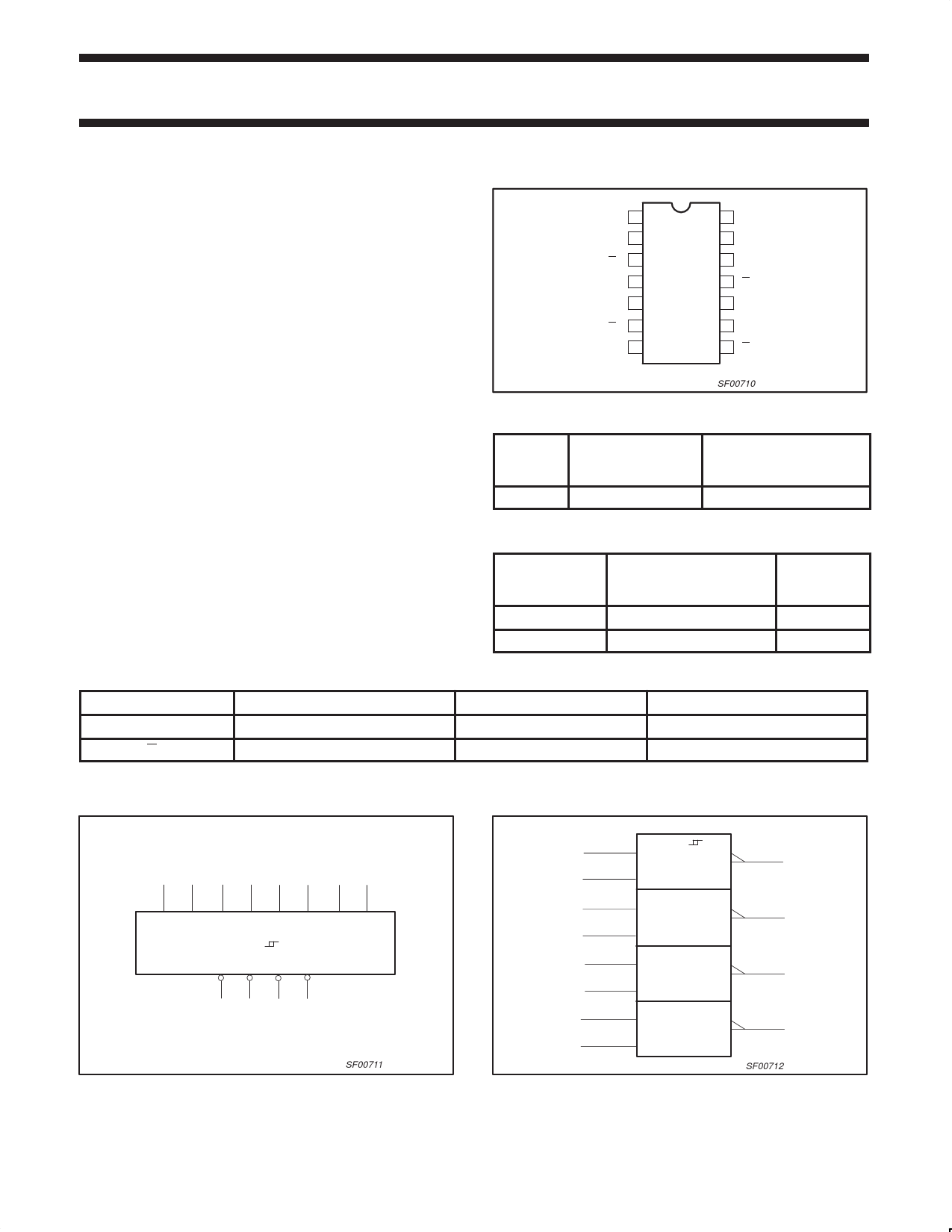
PIN CONFIGURATION
D0a 1
D0b 2
Q0 3
D1a 4
D1b 5
Q1 6
GND 7
14 VCC
13 D3b
12 D3a
11 Q3
10 D2b
9 D2a
8 Q2
SF00710
TYPE
74F132
TYPICAL
PROPAGATION
DELAY
6.3ns
TYPICAL
SUPPLY CURRENT
(TOTAL)
13mA
ORDERING INFORMATION
DESCRIPTION
COMMERCIAL RANGE
VCC = 5V ±10%,
Tamb = 0°C to +70°C
14-pin plastic DIP
N74F132N
14-pin plastic SO
N74F132D
PKG DWG #
SOT27-1
SOT108-1
INPUT AND OUTPUT LOADING AND FAN-OUT TABLE
PINS
DESCRIPTION
74F (U.L.) HIGH/LOW
Dna, Dnb
Data inputs
1.0/1.0
Qn
Data output
50/33
NOTE: One (1.0) FAST unit load is defined as: 20µA in the High state and 0.6mA in the Low state.
LOGIC SYMBOL
IEC/IEEE SYMBOL
LOAD VALUE HIGH/LOW
20µA/0.6mA
1.0mA/20mA
1
2
45
9 10 12 13
D0a D0b D1a D1b D2a D2b D3a D3b
VCC = Pin 14
GND = Pin 7
Q0 Q1 Q2 Q3
3 6 8 11
SF00711
1
&
3
2
4
6
5
9
8
10
12
11
13
SF00712
1991 Jun 26
2
853–0342 03094
Share Link: 