74LV273 데이터 시트보기 (PDF) - Philips Electronics
부품명
상세내역
제조사
74LV273 Datasheet PDF : 12 Pages
| |||
Philips Semiconductors
Octal D-type flip-flop with reset; positive edge-trigger
Product specification
74LV273
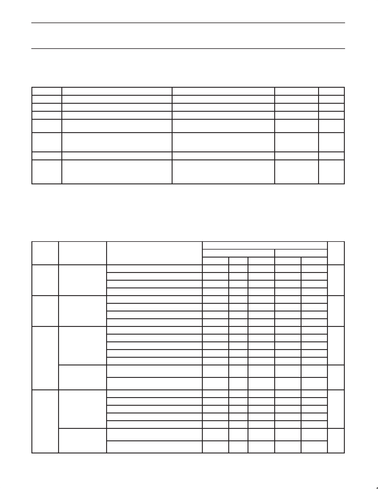
ABSOLUTE MAXIMUM RATINGS1, 2
In accordance with the Absolute Maximum Rating System (IEC 134)
Voltages are referenced to GND (ground = 0V)
SYMBOL
PARAMETER
CONDITIONS
VCC
±IIK
±IOK
±IO
DC supply voltage
DC input diode current
DC output diode current
DC output source or sink current
– standard outputs
VI < –0.5 or VI > VCC + 0.5V
VO < –0.5 or VO > VCC + 0.5V
–0.5V < VO < VCC + 0.5V
RATING
–0.5 to +7.0
20
50
25
UNIT
V
mA
mA
mA
±IGND,
±ICC
DC VCC or GND current for types with
–standard outputs
50
mA
Tstg
Storage temperature range
–65 to +150
°C
Power dissipation per package
for temperature range: –40 to +125°C
PTOT
–plastic DIL
–plastic mini-pack (SO)
above +70°C derate linearly with 12mW/K
above +70°C derate linearly with 8 mW/K
750
500
mW
–plastic shrink mini-pack (SSOP and TSSOP) above +60°C derate linearly with 5.5 mW/K
400
NOTES:
1. Stresses beyond those listed may cause permanent damage to the device. These are stress ratings only and functional operation of the
device at these or any other conditions beyond those indicated under “recommended operating conditions” is not implied. Exposure to
absolute-maximum-rated conditions for extended periods may affect device reliability.
2. The input and output voltage ratings may be exceeded if the input and output current ratings are observed.
DC CHARACTERISTICS FOR THE LV FAMILY
Over recommended operating conditions voltages are referenced to GND (ground = 0V)
LIMITS
SYMBOL PARAMETER
TEST CONDITIONS
-40°C to +85°C
MIN
TYP1 MAX
VCC = 1.2V
0.9
VIH
HIGH level Input
voltage
VCC = 2.0V
VCC = 2.7 to 3.6V
1.4
2.0
VCC = 4.5 to 5.5V
0.7*VCC
VCC = 1.2V
0.3
VIL
LOW level Input
voltage
VCC = 2.0V
VCC = 2.7 to 3.6V
0.6
0.8
VCC = 4.5 to 5.5
0.3*VCC
VCC = 1.2V; VI = VIH or VIL; –IO = 100µA
1.2
VCC = 2.0V; VI = VIH or VIL; –IO = 100µA
1.8
2.0
HIGH level output
voltage; all outputs
VCC = 2.7V; VI = VIH or VIL; –IO = 100µA
2.5
2.7
VOH
VCC = 3.0V; VI = VIH or VIL; –IO = 100µA
2.8
3.0
VCC = 4.5V;VI = VIH or VIL; –IO = 100µA
4.3
4.5
HIGH level output
voltage;
STANDARD
outputs
VCC = 3.0V;VI = VIH or VIL; –IO = 6mA
VCC = 4.5V;VI = VIH or VIL; –IO = 12mA
2.40
2.82
3.60
4.20
VCC = 1.2V; VI = VIH or VIL; IO = 100µA
LOW level output
voltage; all outputs
VCC = 2.0V; VI = VIH or VIL; IO = 100µA
VCC = 2.7V; VI = VIH or VIL; IO = 100µA
VCC = 3.0V;VI = VIH or VIL; IO = 100µA
VOL
VCC = 4.5V;VI = VIH or VIL; IO = 100µA
LOW level output
voltage;
STANDARD
outputs
VCC = 3.0V;VI = VIH or VIL; IO = 6mA
VCC = 4.5V;VI = VIH or VIL; IO = 12mA
0
0
0.2
0
0.2
0
0.2
0
0.2
0.25
0.40
0.35
0.55
-40°C to +125°C
MIN
MAX
0.9
1.4
2.0
0.7*VCC
0.3
0.6
0.8
0.3*VCC
1.8
2.5
2.8
4.3
2.20
3.50
0.2
0.2
0.2
0.2
0.50
0.65
UNIT
V
V
V
V
V
V
1998 May 29
5
Share Link: 