74LV273N 데이터 시트보기 (PDF) - Philips Electronics
부품명
상세내역
제조사
74LV273N Datasheet PDF : 12 Pages
| |||
Philips Semiconductors
Octal D-type flip-flop with reset; positive edge-trigger
Product specification
74LV273
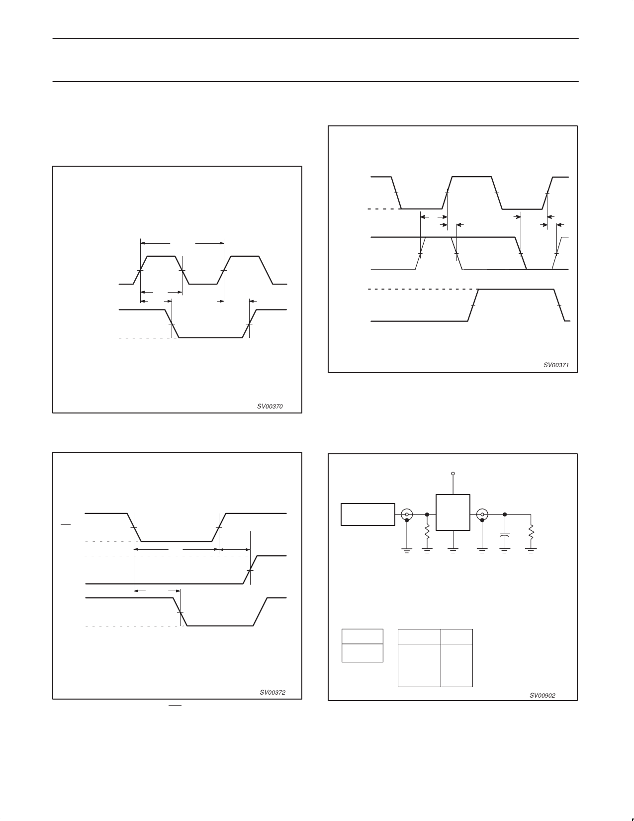
AC WAVEFORMS
VM = 1.5V at VCC w 2.7V v 3.6V
VM = 0.5V * VCC at VCC t 2.7V and w 4.5V
VOL and VOH are the typical output voltage drop that occur with the
output load.
VI
CP INPUT
GND
VOH
Qn OUTPUT
VOL
1/fMAX
VM
tw
tPHL
VM
tPLH
SV00370
Figure 1. The clock (CP) to output (Qn) propagation delays, the
clock pulse width and the maximum clock pulse frequency
VI
CP INPUT
VM
GND
ÌÌÌÌ VI
ÌÌÌÌ Dn INPUT
ÌÌÌÌ GND
tsu
VM
ÌÌÌth ÌÌÌÌÌÌÌÌÌÌÌÌÌÌÌtsu ÌÌÌthÌÌÌ
VOH
Qn OUTPUT
VM
VOL
SV00371
Figure 3. Data set-up and hold times for the data input (Dn)
NOTE:
The shaded areas indicate when the input is permitted to change for
predictable output performance.
TEST CIRCUIT
Vcc
VI
MR INPUT
GND
VI
CP INPUT
GND
VOH
Qn OUTPUT
VOL
VM
VM
tw
tPHL
VM
trem
VM
SV00372
Figure 2. The master reset (MR) pulse width, the master reset
to output (Qn) propagations delay and the master reset to clock
(CP) removal time
PULSE
GENERATOR
Vl
RT
D.U.T.
VO
50pF
CL
RL= 1k
Test Circuit for Outputs
DEFINITIONS
RL = Load resistor
CL = Load capacitance includes jig and probe capacitiance
RT = Termination resistance should be equal to ZOUT of pulse generators.
TEST
tPLH/tPHL
VCC
< 2.7V
2.7–3.6V
≥ 4.5 V
VI
VCC
2.7V
VCC
SV00902
Figure 4. Load circuitry for switching times
1998 May 29
7
Share Link: 