74LVC1G07 데이터 시트보기 (PDF) - Philips Electronics
부품명
상세내역
제조사
74LVC1G07 Datasheet PDF : 15 Pages
| |||
Philips Semiconductors
Buffer with open-drain output
Product specification
74LVC1G07
FEATURES
• Wide supply voltage range from 1.65 V to 5.5 V
• High noise immunity
• Complies with JEDEC standard:
– JESD8-7 (1.65 V to 1.95 V)
– JESD8-5 (2.3 V to 2.7 V)
– JESD8B/JESD36 (2.7 V to 3.6 V).
• 24 mA output drive (VCC = 3.0 V)
• CMOS low power consumption
• Latch-up performance exceeds 250 mA
• Direct interface with TTL levels
• Inputs accept voltages up to 5 V
• Multiple package options
• ESD protection:
– HBM EIA/JESD22-A114-B exceeds 2000 V
– MM EIA/JESD22-A115-A exceeds 200 V.
• Specified from −40 °C to +85 °C and −40 °C to +125 °C.
DESCRIPTION
The 74LVC1G07 is a high-performance, low-power,
low-voltage, Si-gate CMOS device, superior to most
advanced CMOS compatible TTL families.
The input can be driven from either 3.3 V or 5 V devices.
This feature allows the use of this device as translator in a
mixed 3.3 V and 5 V environment.
Schmitt trigger action at the input makes the circuit tolerant
for slower input rise and fall time.
The 74LVC1G07 provides the non-inverting buffer.
The output of the device is an open drain and can be
connected to other open-drain outputs to implement
active-LOW wired-OR or active-HIGH wired-AND
functions.
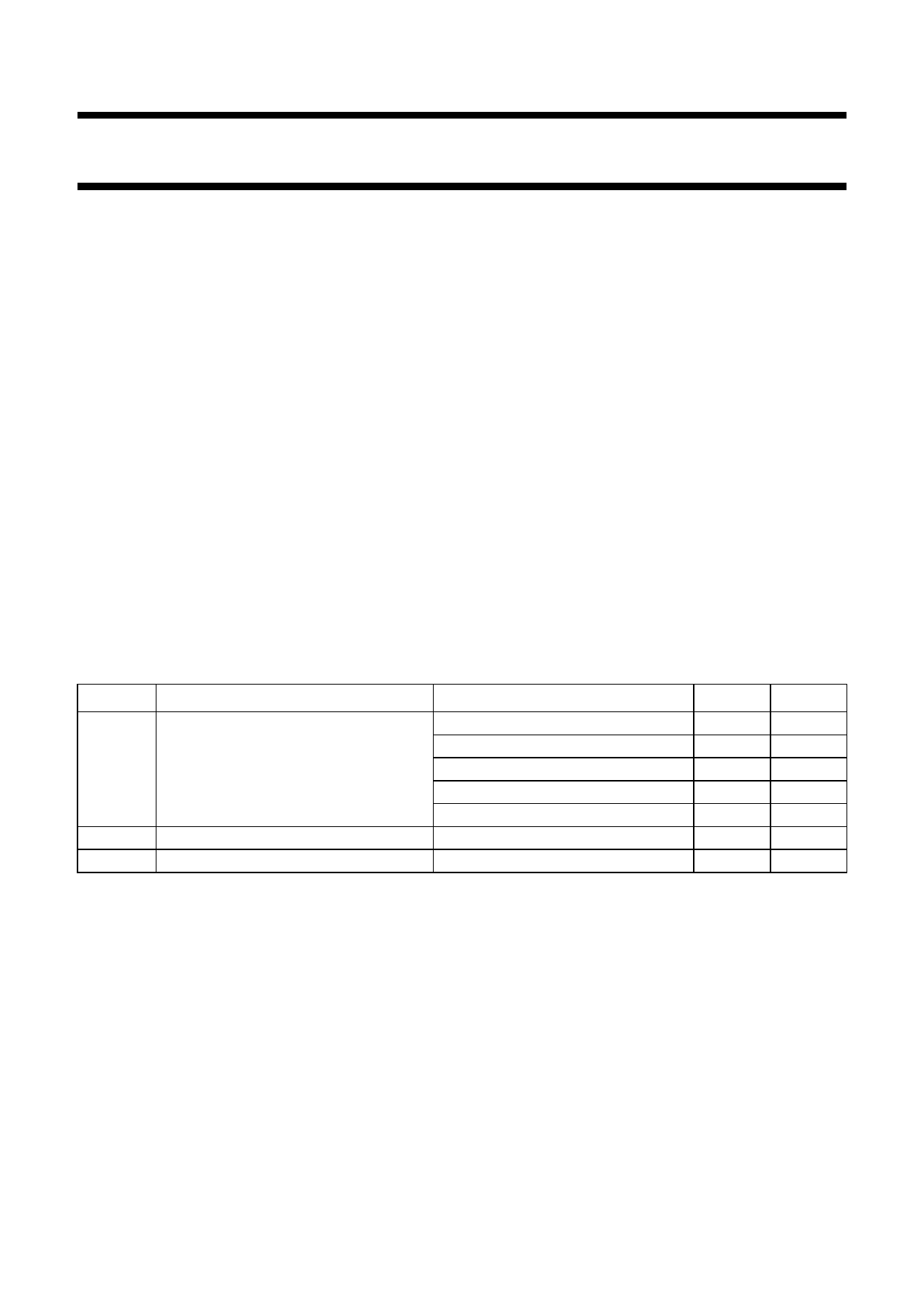
QUICK REFERENCE DATA
GND = 0 V; Tamb = 25 °C; tr = tf ≤ 2.5 ns.
SYMBOL
PARAMETER
tPLZ/tPZL propagation delay inputs A to output Y
CI
input capacitance
CPD
power dissipation capacitance per gate
CONDITIONS
VCC = 1.8 V; CL = 30 pF; RL = 1 kΩ
VCC = 2.5 V; CL = 30 pF; RL = 500 Ω
VCC = 2.7 V; CL = 50 pF; RL = 500 Ω
VCC = 3.3 V; CL = 50 pF; RL = 500 Ω
VCC = 5.0 V; CL = 50 pF; RL = 500 Ω
VCC = 3.3 V; notes 1 and 2
Notes
1. CPD is used to determine the dynamic power dissipation (PD in µW).
PD = CPD × VCC2 × fi × N + Σ(CL × VCC2 × fo) where:
fi = input frequency in MHz;
fo = output frequency in MHz;
CL = output load capacitance in pF;
VCC = supply voltage in Volts;
N = total load switching outputs;
Σ(CL × VCC2 × fo) = sum of the outputs.
2. The condition is VI = GND to VCC.
TYPICAL UNIT
2.6
ns
1.7
ns
2.3
ns
2.2
ns
1.6
ns
5
pF
7
pF
2004 Sep 07
2
Share Link: 