74LVC1G19 데이터 시트보기 (PDF) - Philips Electronics
부품명
상세내역
제조사
74LVC1G19 Datasheet PDF : 14 Pages
| |||
Philips Semiconductors
1-of-2 decoder/demultiplexer
Product specification
74LVC1G19
FEATURES
• Wide supply voltage range from 1.65 V to 5.5 V
• 5 V tolerant inputs for interfacing with 5 V logic
• High noise immunity
• Complies with JEDEC standard:
– JESD8-7 (1.65 V to 1.95 V)
– JESD8-5 (2.3 V to 2.7 V)
– JESD8B/JESD36 (2.7 V to 3.6 V).
• ESD protection:
– HBM EIA/JESD22-A114-B exceeds 2000 V
– MM EIA/JESD22-A115-A exceeds 200 V.
• ±24 mA output drive (VCC = 3.0 V)
• CMOS low power consumption
• Latch-up performance exceeds 250 mA
• Direct interface with TTL levels
• Multiple package options
• Specified from −40 °C to +85 °C and
−40 °C to +125 °C.
DESCRIPTION
The 74LVC1G19 is a high-performance, low-power,
low-voltage, Si-gate CMOS device, superior to most
advanced CMOS compatible TTL families.
Input can be driven from either 3.3 V or 5 V devices.
These features allow the use of these devices in a mixed
3.3 V and 5 V environment.
This device is fully specified for partial power-down
applications using Ioff. The Ioff circuitry disables the output,
preventing the damaging backflow current through the
device when it is powered down.
The 74LVC1G19 is a 1-of-2 decoder/demultiplexer with a
common output enable. The 74LVC1G19 buffers the data
on input pin E and passes it either to output pin 1Y or 2Y,
depending on whether the state of the select input pin A is
LOW or HIGH, respectively.
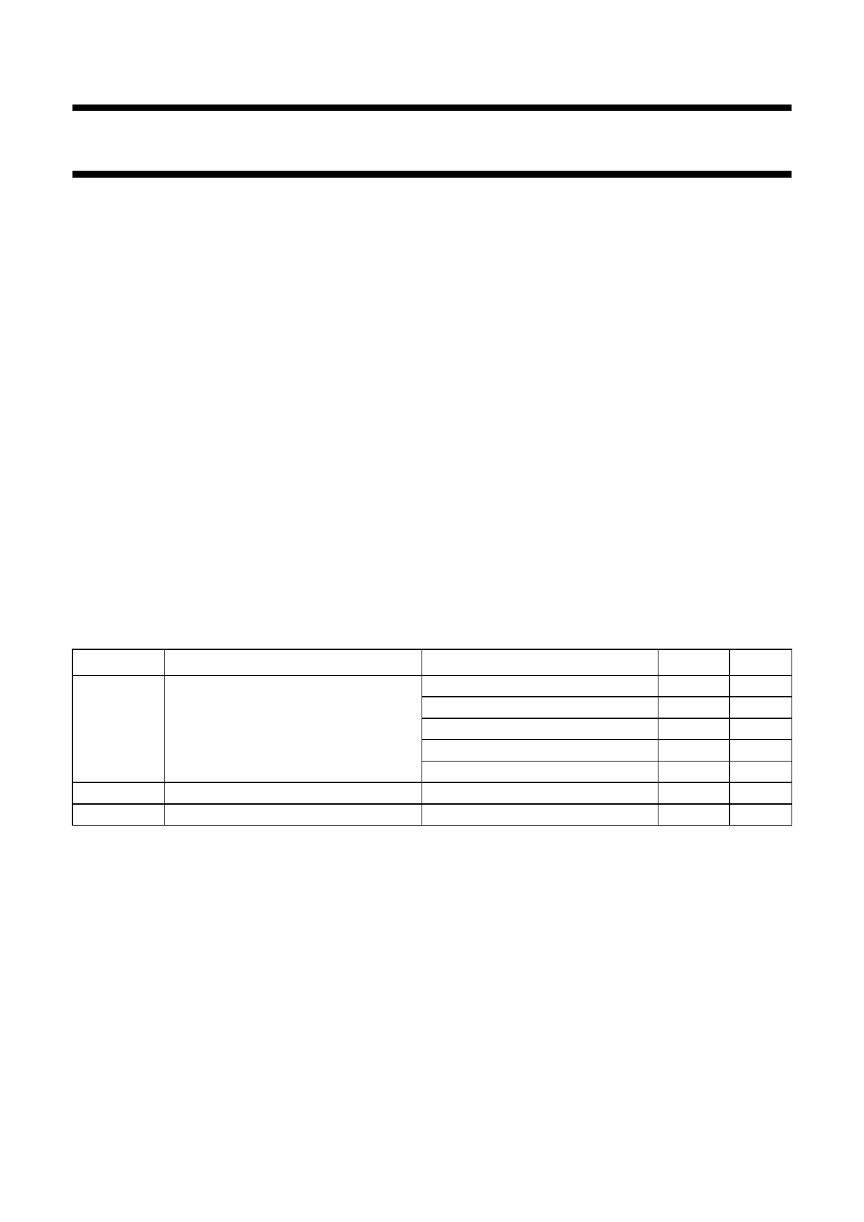
QUICK REFERENCE DATA
GND = 0 V; Tamb = 25 °C.
SYMBOL
tPHL/tPLH
CI
CPD
PARAMETER
propagation delay input A to output nY
input capacitance
power dissipation capacitance
CONDITIONS
VCC = 1.8 V; CL = 30 pF; RL = 1 kΩ
VCC = 2.5 V; CL = 30 pF; RL = 500 Ω
VCC = 2.7 V; CL = 50 pF; RL = 500 Ω
VCC = 3.3 V; CL = 50 pF; RL = 500 Ω
VCC = 5.0 V; CL = 50 pF; RL = 500 Ω
VCC = 3.3 V; notes 1 and 2
TYPICAL UNIT
4.0
ns
2.5
ns
2.8
ns
2.5
ns
1.8
ns
2.5
pF
18.9
pF
Notes
1. CPD is used to determine the dynamic power dissipation (PD in µW).
PD = CPD × VCC2 × fi × N + ∑(CL × VCC2 × fo) where:
fi = input frequency in MHz;
fo = output frequency in MHz;
CL = output load capacitance in pF;
VCC = supply voltage in Volts;
N = number of inputs switching;
∑(CL × VCC2 × fo) = sum of outputs.
2. The condition is VI = GND to VCC.
2004 Oct 18
2
Share Link: 