74LVC27 데이터 시트보기 (PDF) - Philips Electronics
부품명
상세내역
제조사
74LVC27 Datasheet PDF : 10 Pages
| |||
Philips Semiconductors
Triple 3-input NOR gate
Product specification
74LVC27
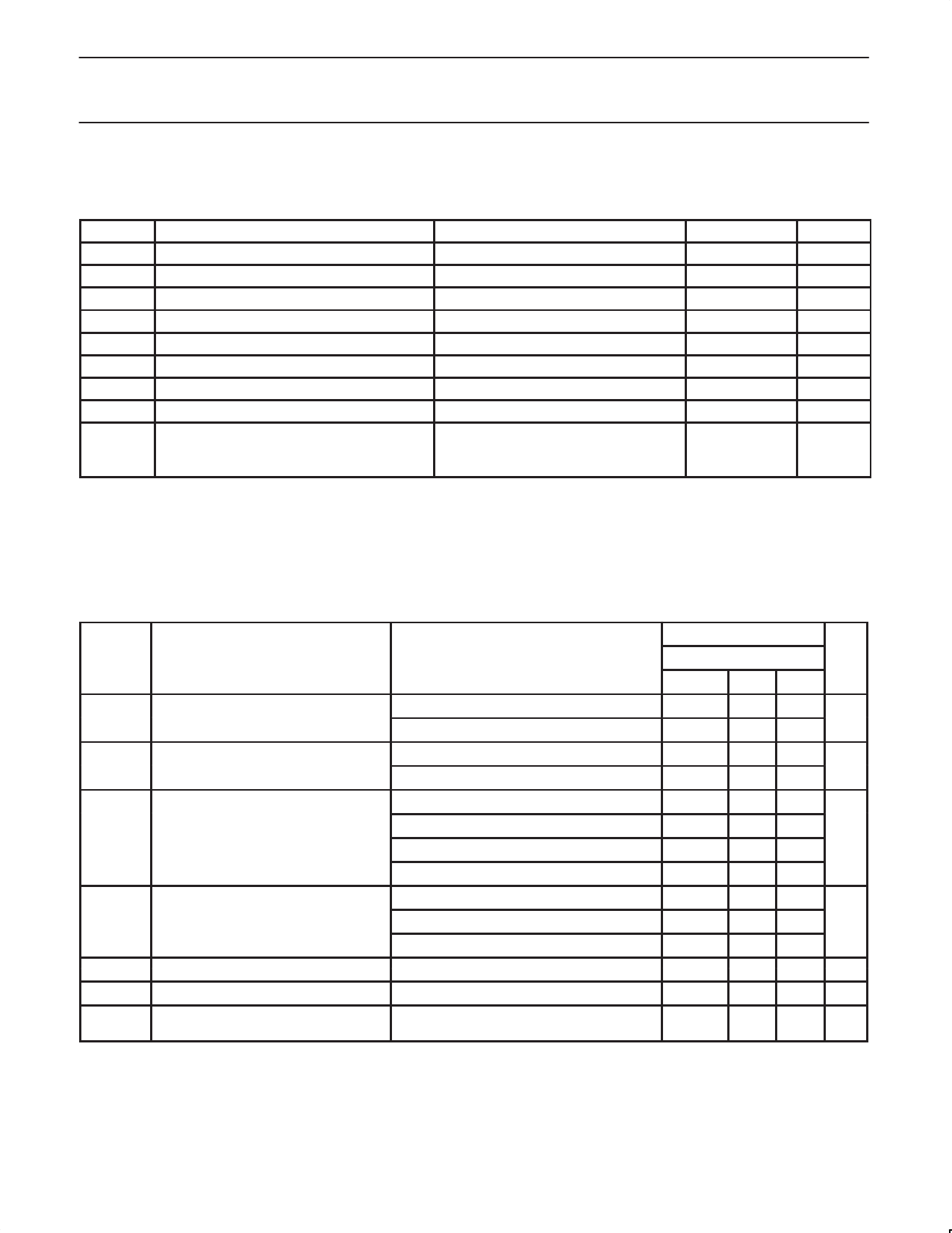
ABSOLUTE MAXIMUM RATINGS1
In accordance with the Absolute Maximum Rating System (IEC 134)
Voltages are referenced to GND (ground = 0V)
SYMBOL
PARAMETER
CONDITIONS
RATING
UNIT
VCC
DC supply voltage
–0.5 to +6.5
V
IIK
DC input diode current
VI t 0
–50
mA
VI
DC input voltage
Note 2
–0.5 to +5.5
V
IOK
DC output diode current
VO uVCC or VO t 0
"50
mA
VO
DC output voltage
Note 2
–0.5 to VCC +0.5
V
IO
DC output source or sink current
VO = 0 to VCC
"50
mA
IGND, ICC DC VCC or GND current
"100
mA
Tstg
Storage temperature range
–60 to +150
°C
Power dissipation per package
PTOT – plastic mini-pack (SO)
above +70°C derate linearly with 8 mW/K
500
– plastic shrink mini-pack (SSOP and TSSOP) above +60°C derate linearly with 5.5 mW/K
500
mW
NOTES:
1. Stresses beyond those listed may cause permanent damage to the device. These are stress ratings only and functional operation of the
device at these or any other conditions beyond those indicated under “recommended operating conditions” is not implied. Exposure to
absolute-maximum-rated conditions for extended periods may affect device reliability.
2. The input and output voltage ratings may be exceeded if the input and output current ratings are observed.
DC ELECTRICAL CHARACTERISTICS
Over recommended operating conditions voltages are referenced to GND (ground = 0V)
SYMBOL
PARAMETER
TEST CONDITIONS
VIH
HIGH level Input voltage
VCC = 1.2V
VCC = 2.7 to 3.6V
VIL
LOW level Input voltage
VCC = 1.2V
VCC = 2.7 to 3.6V
VCC = 2.7V; VI = VIH or VIL; IO = –12mA
VOH HIGH level output voltage
VCC = 3.0V; VI = VIH or VIL; IO = –100µA
VCC = 3.0V; VI = VIH or VIL; IO = –12mA
VCC = 3.0V; VI = VIH or VIL; IO = –24mA
VCC = 2.7V; VI = VIH or VIL; IO = 12mA
VOL LOW level output voltage
VCC = 3.0V; VI = VIH or VIL; IO = 100µA
VCC = 3.0V; VI = VIH or VIL; IO = 24mA
II
Input leakage current
VCC = 3.6V; VI = 5.5V or GND
ICC
Quiescent supply current
VCC = 3.6V; VI = VCC or GND; IO = 0
∆ICC
Additional quiescent supply current per
input pin
VCC = 2.7V to 3.6V; VI = VCC –0.6V; IO = 0
NOTE:
1. All typical values are at VCC = 3.3V and Tamb = 25°C.
LIMITS
Temp = -40°C to +85°C
MIN
TYP1 MAX
VCC
2.0
GND
0.8
VCC*0.5
VCC*0.2 VCC
VCC*0.6
VCC*1.0
0.40
GND 0.20
0.55
"0.1 "5
0.1
10
UNIT
V
V
V
V
µA
µA
5
500 µA
1998 Apr 28
4
Share Link: 