ACPL-332J 데이터 시트보기 (PDF) - Avago Technologies
부품명
상세내역
제조사
ACPL-332J Datasheet PDF : 24 Pages
| |||
ACPL-332J
2.5 Amp Output Current IGBT Gate Driver Optocoupler
with Integrated (VCE) Desaturation Detection, UVLO
Fault Status Feedback and Active Miller Clamping
Data Sheet
Lead (Pb) Free
RoHS 6 fully
compliant
RoHS 6 fully compliant options available;
-xxxE denotes a lead-free product
Description
Features
The ACPL-332J is an advanced 2.5 A output current, easy-
to-use, intelligent gate driver which makes IGBT VCE fault
protection compact, affordable, and easy-to implement.
Features such as integrated VCE detection, under
voltage lockout (UVLO), “soft” IGBT turn-off, isolated
open collector fault feedback and active Miller clamping
provide maximum design flexibility and circuit protec-
tion.
The ACPL-332J contains a GaAsP LED. The LED is optically
coupled to an integrated circuit with a power output
stage. ACPL-332J is ideally suited for driving power IGBTs
and MOSFETs used in motor control inverter applications.
The voltage and current supplied by these optocouplers
make them ideally suited for directly driving IGBTs with
ratings up to 1200 V and 150 A. For IGBTs with higher
ratings, the ACPL-332J can be used to drive a discrete
power stage which drives the IGBT gate. The ACPL-332J
has an insulation voltage of VIORM = 891 VPEAK.
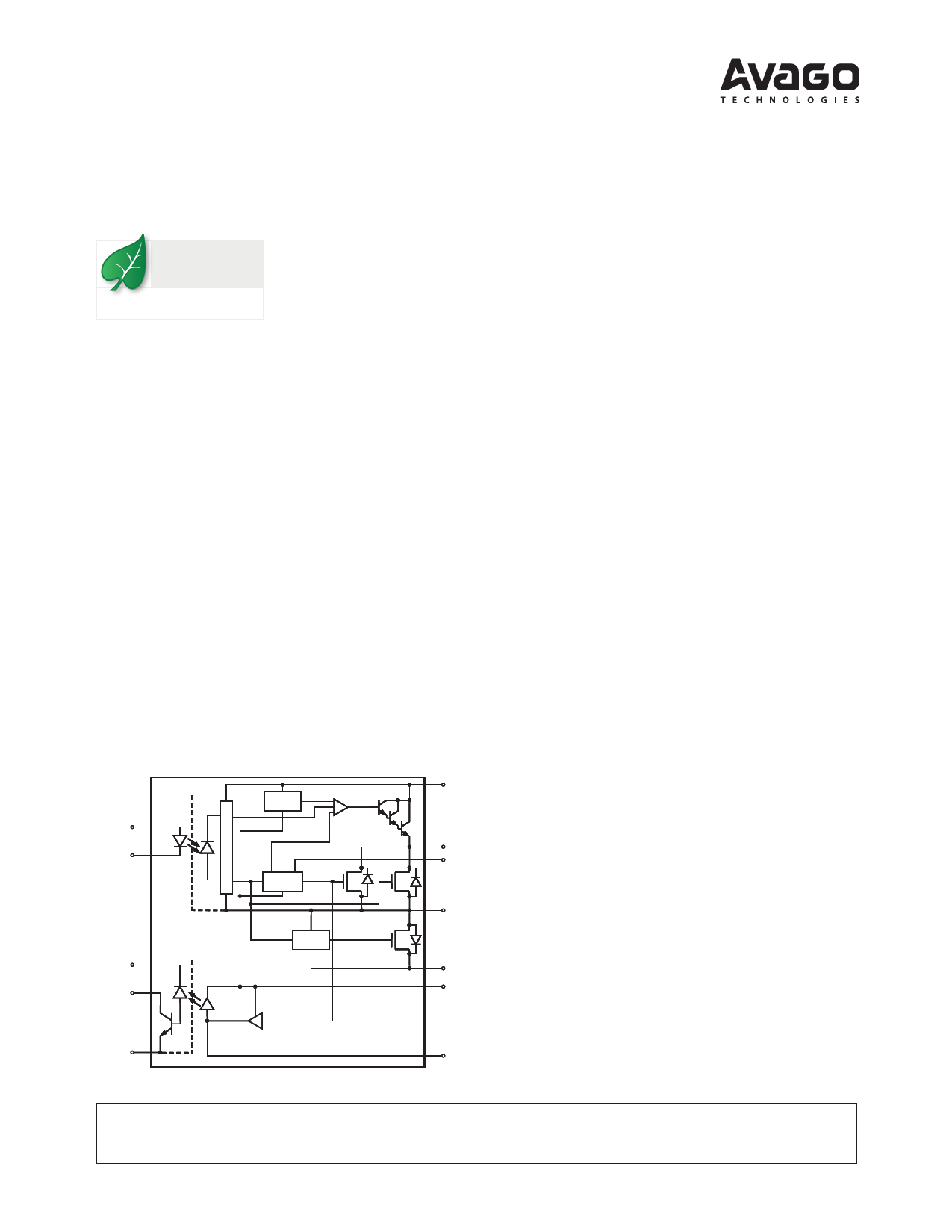
Block Diagram
6, 7
D
ANODE
R
5, 8
I
CATHODE
V
LED1
E
R
2
VCC1
3
FAULT
SHIELD
LED2
UVLO
DESAT
VCLAMP
13
VCC2
11
VOUT
DESAT
14
9, 12
VEE
10
VCLAMP
VE
16
1, 4
VS
SHIELD
15
VLED
• Under Voltage Lock-Out Protection (UVLO) with
Hysteresis
• Desaturation Detection
• Miller Clamping
• Open Collector Isolated fault feedback
• “Soft” IGBT Turn-off
• Fault Reset by next LED turn-on (low to high) after
fault mute period
• Available in SO-16 package
• Safety approvals: UL approved, 3750 VRMS for 1
minute, CSA approved, IEC/EN/DIN-EN 60747-5-2
approved VIORM = 891 VPEAK
Specifications
• 2.5 A maximum peak output current
• 2.0 A minimum peak output current
• 250 ns maximum propagation delay over temperature
range
• 100 ns maximum pulse width distortion (PWD)
• 15 kV/µs minimum common mode rejection (CMR) at
VCM = 1500 V
• ICC(max) < 5 mA maximum supply current
• Wide VCC operating range: 15 V to 30 V over
temperature range
• 1.7 A Miller Clamp. Clamp pin short to VEE if not used
• Wide operating temperature range: –40°C to 105°C
Applications
• Isolated IGBT/Power MOSFET gate drive
• AC and brushless DC motor drives
• Industrial inverters and Uninterruptible Power Supply
(UPS)
CAUTION: It is advised that normal static precautions be taken in handling and assembly
of this component to prevent damage and/or degradation which may be induced by ESD.
Share Link: 