ACPM-7392 데이터 시트보기 (PDF) - Avago Technologies
부품명
상세내역
제조사
ACPM-7392 Datasheet PDF : 18 Pages
| |||
Application on mobile phone board
Application example in mobile is shown below. C4 and C5
should be placed close to pin1 and pin10. Bypass cap C1,
C2 and C3 should be also placed nearby from pin5, pin4
and pin3, respectively. The length of post-PA transmission
line should be minimized to reduce line loss.
PCB layout and part placement on phone board
3
1
2
V BATT
C6
RF In
BB
C4
C9
C3
PA_R1
PA_R0
PA_ON
Vcc1
Vcc2
IN
GND
V bp
OUT
Vmode GND
Ven
GND
ACPM-7392
C2
C1
C5
output matching circuit
C8
C7
L1
Peripheral Circuits
4
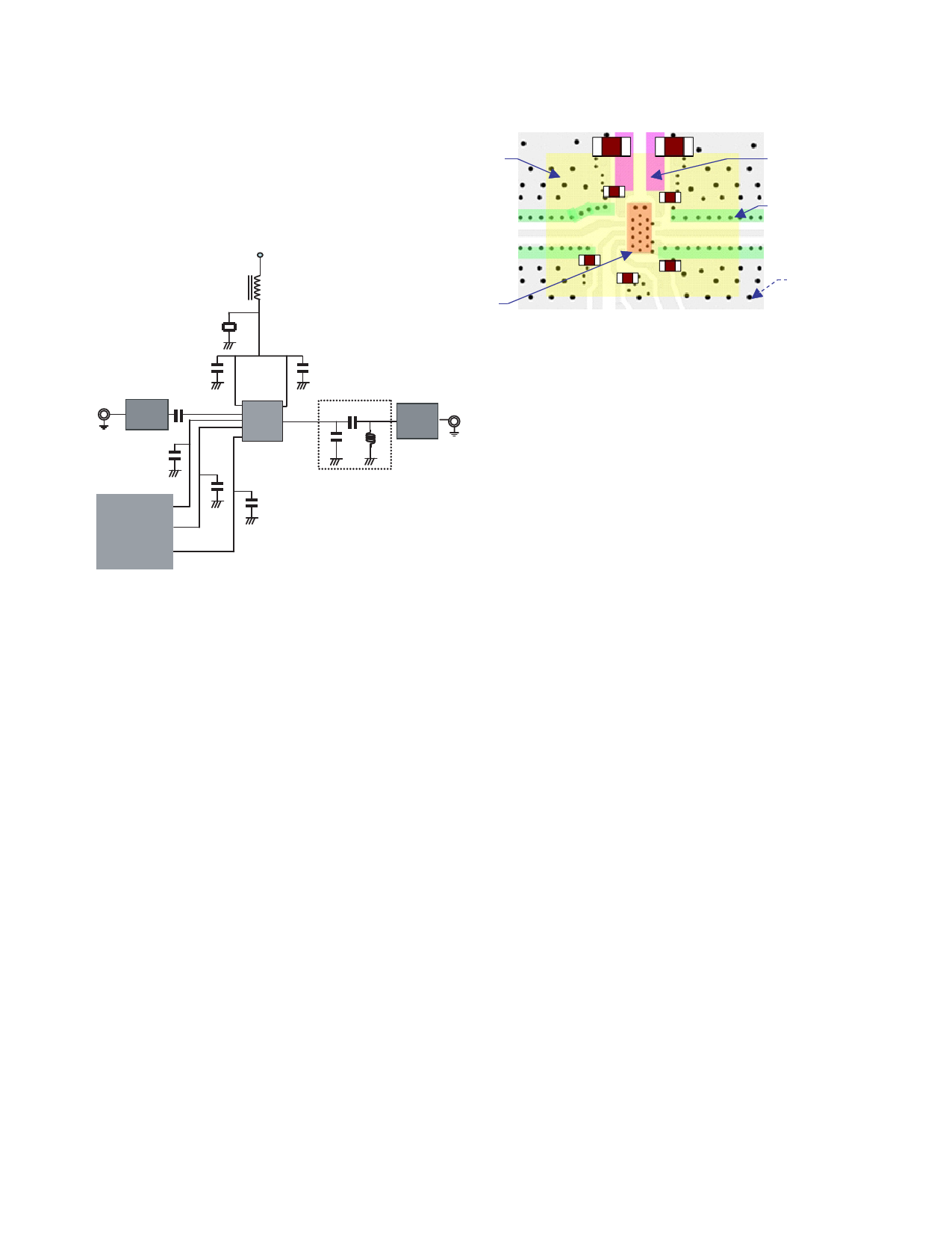
PCB guideline on phone board
Via hole
Notes
1. To prevent voltage drop, make the bias lines as wide as
possible (Pink line).
RF Out 2. Use many via holes to fence off PA RF input and output
traces for better isolation. Output signal of the PA
should be isolated from input signal and the receive
signal. Output signal should not be fed into PA input.
(Green line)
3. Use via holes to connect outer ground plates to internal
ground planes. They help heat spread out more easily
and accordingly the board temperature can be lowered.
They also help to improve RF stability (Yellow square).
4. PA which has a ground slug requires many via holes
which go through all the layers (Red square).
Share Link: 