ACS8520A 데이터 시트보기 (PDF) - Semtech Corporation
부품명
상세내역
제조사
ACS8520A Datasheet PDF : 150 Pages
| |||
ACS8520A SETS
Synchronous Equipment Timing Source for
Stratum 3/4E/4 and SMC Systems
ADVANCED COMMSUN&ICSAETNIOSNINSG
Description
FINAL
Features
DATASHEET
The ACS8520A is a highly integrated, single-chip solution
for the Synchronous Equipment Timing Source (SETS)
function in a SONET or SDH Network Element. The device
generates SONET or SDH Equipment Clocks (SEC) and
Frame Synchronization clocks. The ACS8520A is fully
compliant with the required international specifications
and standards.
The device supports Free-run, Locked and Holdover
modes. It also supports all three types of reference clock
source: recovered line clock, PDH network, and node
synchronization. The ACS8520A generates independent
SEC and BITS/SSU clocks, an 8 kHz Frame
Synchronization clock and a 2 kHz Multi-Frame
Synchronization clock.
Two ACS8520A devices can be used together in a Master/
Slave configuration mode allowing system protection
against a single ACS8520A failure.
A microprocessor port is incorporated, providing access to
the configuration and status registers for device setup
and monitoring. The ACS8520A supports IEEE 1149.1[5]
JTAG boundary scan.
The user can choose between OCXO or TCXO to define the
Stratum and/or Holdover performance required.
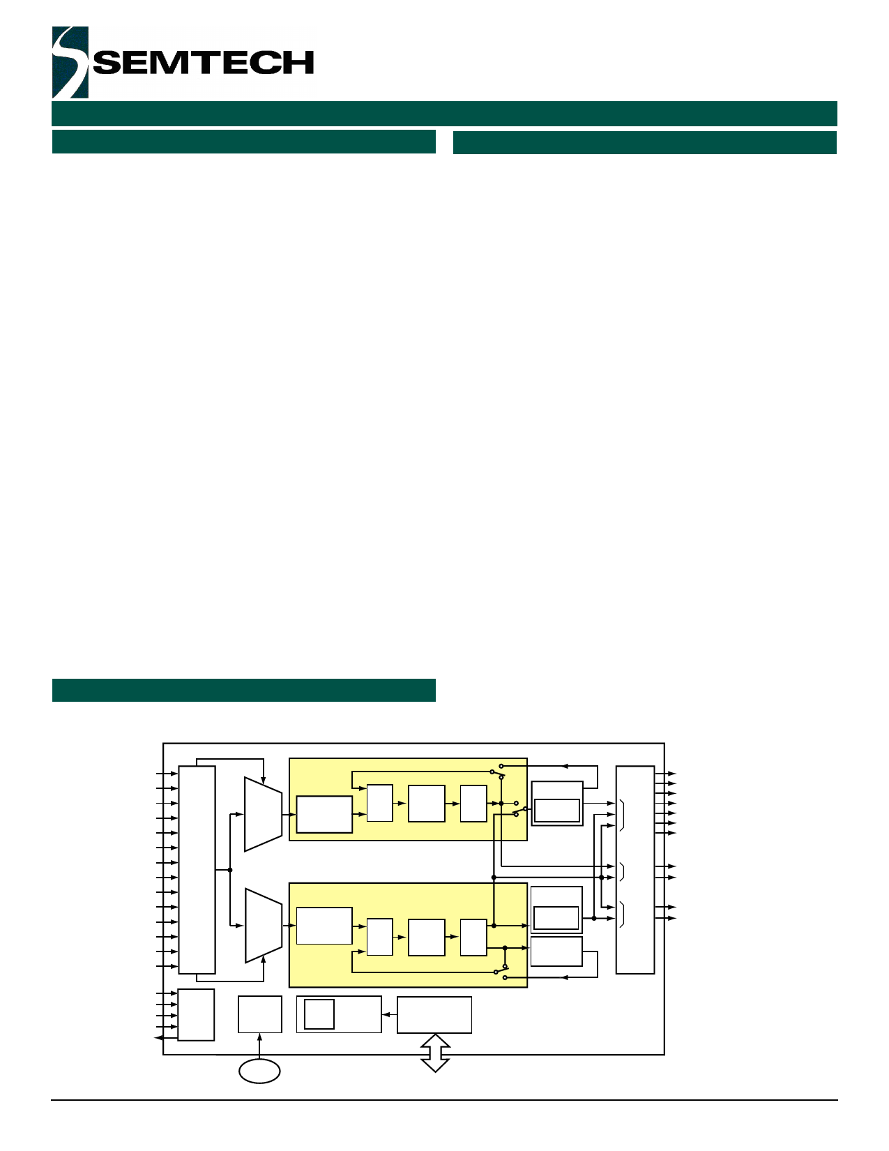
Block Diagram
Suitable for Stratum 3, 4E, 4 and SONET Minimum
Clock (SMC) or SONET/SDH Equipment Clock (SEC)
applications
Meets Telcordia 1244-CORE[19] Stratum 3 and
GR-253[17], and ITU-T G.813[11] Options Ι and ΙΙ
specifications
Accepts 14 individual input reference clocks, all with
robust input clock source quality monitoring.
Simultaneously generates nine output clocks, plus
two Sync pulse outputs
Absolute Holdover accuracy better than 3 x 10⁻¹⁰
(manual), 7.5 x 10⁻¹⁴ (instantaneous); Holdover
stability defined by choice of external XO
Programmable PLL bandwidth, for wander and jitter
tracking/attenuation, 0.1 Hz to 70 Hz in 10 steps
Automatic hit-less source switchover on loss of input
Microprocessor interface - Intel, Motorola, Serial,
Multiplexed, or boot from EPROM
Output phase adjustment in 6 ps steps up to ±200 ns
IEEE 1149.1 JTAG Boundary Scan
Single 3.3 V operation
Available in LQFP 100 package
Lead (Pb) - free version available (ACS8520AT), RoHS
and WEEE compliant.
Figure 1 Block Diagram of the ACS8520A SETS
2 x AMI
10 x TTL
2 x PECL/LVDS
Programmable;
64/8 kHz (AMI)
2 kHz
4 kHz
N x 8 kHz
1.544/2.048 MHz
6.48 MHz
19.44 MHz
25.92 MHz
38.88 MHz
51.84 MHz
77.76 MHz
155.52 MHz
Input
Port
Monitors
and
Selection
Control
14 x SEC
T4 DPLL/Freq. Synthesis
Digital
T4
Optional
PFD
Selector
Divider, 1/n
n = 1 to 214
Loop
Filter
DTO
T0 DPLL/Freq. Synthesis
T0
Optional
Selector
Divider, 1/n
n = 1 to 214
PFD
Digital
Loop
DTO
Filter
TCK
TDI
TMS
TRST
TDO
IEEE
1149.1
JTAG
Chip
Clock
Generator
Priority Register Set
Table
OCXO or
TCXO
Revision 1.00/September 2007© Semtech Corp.
Microprocessor
Port
Page 1
T4 APLL
Frequency
Dividers
T0 APLL
(output)
Frequency
Dividers
TO APLL
(feedback)
Output
Ports
TO1
to
TO7
TO8
&
TO9
TO10
&
TO11
Outputs
T01-TO7:
E1/DS1 (2.048/
1.544 MHz)
and frequency
multiples:
1.5 x, 2 x, 3 x
4 x, 6 x, 12 x
16 x and 24 x
E3/DS3
2 kHz
8 kHz
and OC-N* rates
T08: AMI
TO9: E1/DS1
TO10: 8 kHz
(FrSync)
TO11: 2 kHz
(MFrSync)
OC-N* rates =
OC-1 51.84 MHz
OC-3 155.52 MHz
and derivatives:
6.48 MHz
19.44 MHz
25.92 MHz
38.88 MHz
51.84 MHz
77.76 MHz
155.52 MHz
311.04 MHz
F8520P_001BLOCKDIA_03
www.semtech.com
Share Link: 