ACS8522 데이터 시트보기 (PDF) - Semtech Corporation
부품명
상세내역
제조사
ACS8522 Datasheet PDF : 118 Pages
| |||
ACS8522 SETS LITE
ADVANCED COMMUNICATIONS
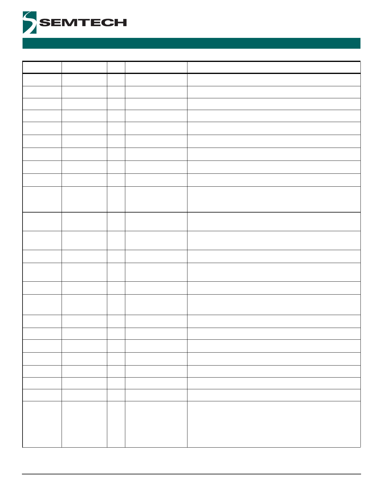
Table 3 Other Pins (cont...)
FINAL
DATASHEET
Pin Number
Symbol
I/O
13
SRCSW
I
17
18
19, 20
28
FrSync
O
MFrSync
O
O1POS, O1NEG O
SYNC2K
I
29
SEC1
I
30
SEC2
I
33
SEC3
I
34
SEC4
I
37
TRST
I
41
TMS
I
42
CLKE
I
43
SDI
I
44
CSB
I
47
SCLK
I
48
PORB
I
Type
TTLD
TTL/CMOS
TTL/CMOS
LVDS/PECL
TTLD
TTLD
TTLD
TTLD
TTLD
TTLD
TTLD
TTLD
TTLD
TTLU
TTLD
TTLU
Description
Source Switching: Force Fast Source Switching on SEC1 and SEC2.
Output Reference: 8 kHz Frame Sync output.
Output Reference: 2 kHz Multi-Frame Sync output.
Output Reference: Programmable, default 38.88 MHz, LVDS.
Multi-Frame Sync 2kHz input.
Input Reference: Programmable, default 8 kHz.
Input Reference: Programmable, default 8 kHz.
Input Reference: Programmable, default 19.44 kHz.
Input Reference: Programmable, default 19.44 kHz.
JTAG Control Reset Input: TRST = 1 to enable JTAG Boundary Scan
mode. TRST = 0 for Boundary Scan stand-by mode, still allowing correct
device operation. If not used connect to GND or leave floating.
JTAG Test Mode Select: Boundary Scan enable. Sampled on rising edge
of TCK. If not used connect to VDD or leave floating.
SCLK Edge Select: SCLK active edge select, CLKE = 1, selects falling
edge of SCLK to be active.
Microprocessor Interface Address: Serial Data Input.
Chip Select (Active Low): This pin is asserted Low by the microprocessor
to enable the microprocessor interface.
Serial Data Clock. When this pin goes High data is latched from SDI pin.
Power-On Reset: Master reset. If PORB is forced Low, all internal states
are reset back to default values.
49
TCK
I
TTLD
JTAG Clock: Boundary Scan clock input.
50
TDO
O
TTL/CMOS
JTAG Output: Serial test data output. Updated on falling edge of TCK.
51
TDI
I
TTLD
JTAG Input: Serial test data Input. Sampled on rising edge of TCK.
52
SDO
O
TTLD
Interface Address: SPI compatible Serial Data Output.
55
O2
O
TTL/CMOS
Output Reference 2: Programmable, default 38.88 MHz.
56
O3
O
TTL/CMOS
Output Reference 3: Programmable, default 19.44 MHz.
59
O4
O
TTL/CMOS
Output Reference 4: Programmable, default 1.544/2.048 MHz (BITS).
64
SONSDHB
I
TTLD
SONET or SDH Frequency Select: Sets the initial power-up state (or state
after a PORB) of the SONET/SDH frequency selection registers, Reg. 34
Bit 2, and Reg. 38 Bits 5 and 6. When set Low, SDH rates are selected
(2.048 MHz etc.), and when set High, SONET rates are selected (1.544
MHz etc.). The register states can be changed after power-up by
software.
Revision 5/November 2006 © Semtech Corp.
Page 6
www.semtech.com
Share Link: 