5962-9089401MEA 데이터 시트보기 (PDF) - Analog Devices
부품명
상세내역
제조사
5962-9089401MEA Datasheet PDF : 14 Pages
| |||
AD526
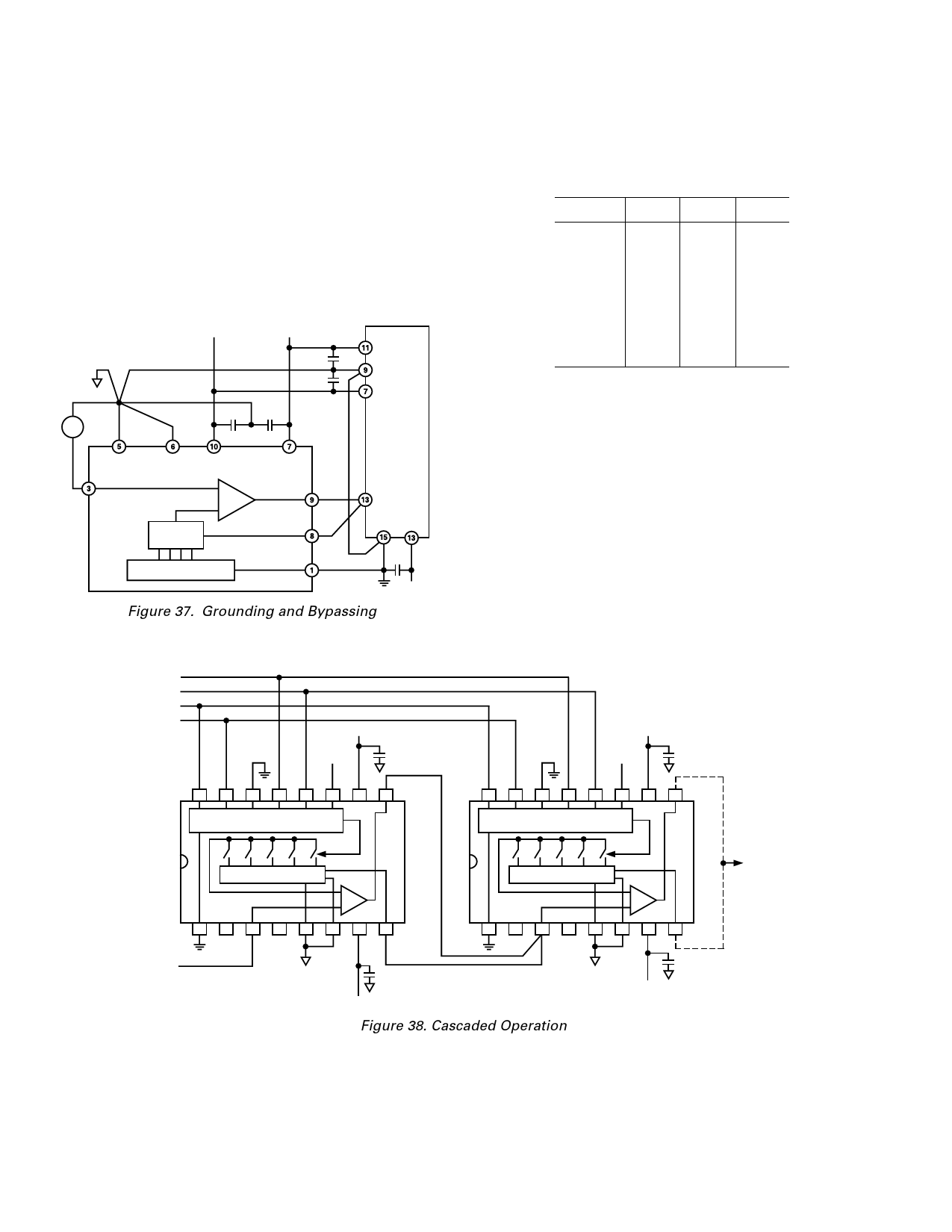
GROUNDING AND BYPASSING
Proper signal and grounding techniques must be applied in
board layout so that specified performance levels of precision
data acquisition components, such as the AD526, are not
degraded.
As is shown in Figure 37, logic and signal grounds should be
separate. By connecting the signal source ground locally to the
AD526 analog ground Pins 5 and 6, gain accuracy of the
AD526 is maintained. This ground connection should not be
corrupted by currents associated with other elements within the
system.
+15V
–15V
0.1F
0.1F
VIN
0.1F 0.1F
ANALOG ANALOG +VS
GROUND 1 GROUND 2
AD526
GAIN
NETWORK
AMP
LATCHES AND LOGIC
–VS
VOUT
FORCE
VOUT
SENSE
DIGITAL
GROUND
AD574
12-BIT
A/D
CONVERTER
1F
+5V
Figure 37. Grounding and Bypassing
Utilizing the force and sense outputs of the AD526, as shown in
Figure 38, avoids signal drops along etch runs to low impedance
loads.
Table II. Logic Table for Figure 38
VOUT/VIN A2
A1
A0
1
0
0
0
2
0
0
1
4
0
1
0
8
0
1
1
16
1
0
0
32
1
0
1
64
1
1
0
128
1
1
1
CLK
A2
A1
A0
+VS
+5V
0.1F
+VS
+5V
0.1F
16 15 14 13 12 11 10
A1 A0 CS CLK A2 B
LOGIC AND LATCHES
16 8 4 2 1
OUT
9 FORCE
16 15 14 13 12 11 10
A1 A0 CS CLK A2 B
LOGIC AND LATCHES
16 8 4 2 1
OUT
9 FORCE
GAIN NETWORK
–
AD526
+
GAIN NETWORK
–
AD526
+
1 2 3 4 5 6 7 8 OUT
SENSE
1 2 3 4 5 6 7 8 OUT
SENSE
VIN
0.1F
–VS
0.1F
–VS
Figure 38. Cascaded Operation
VOUT
–10–
REV. D
Share Link: 