AD5539 데이터 시트보기 (PDF) - Analog Devices
부품명
상세내역
제조사
AD5539 Datasheet PDF : 16 Pages
| |||
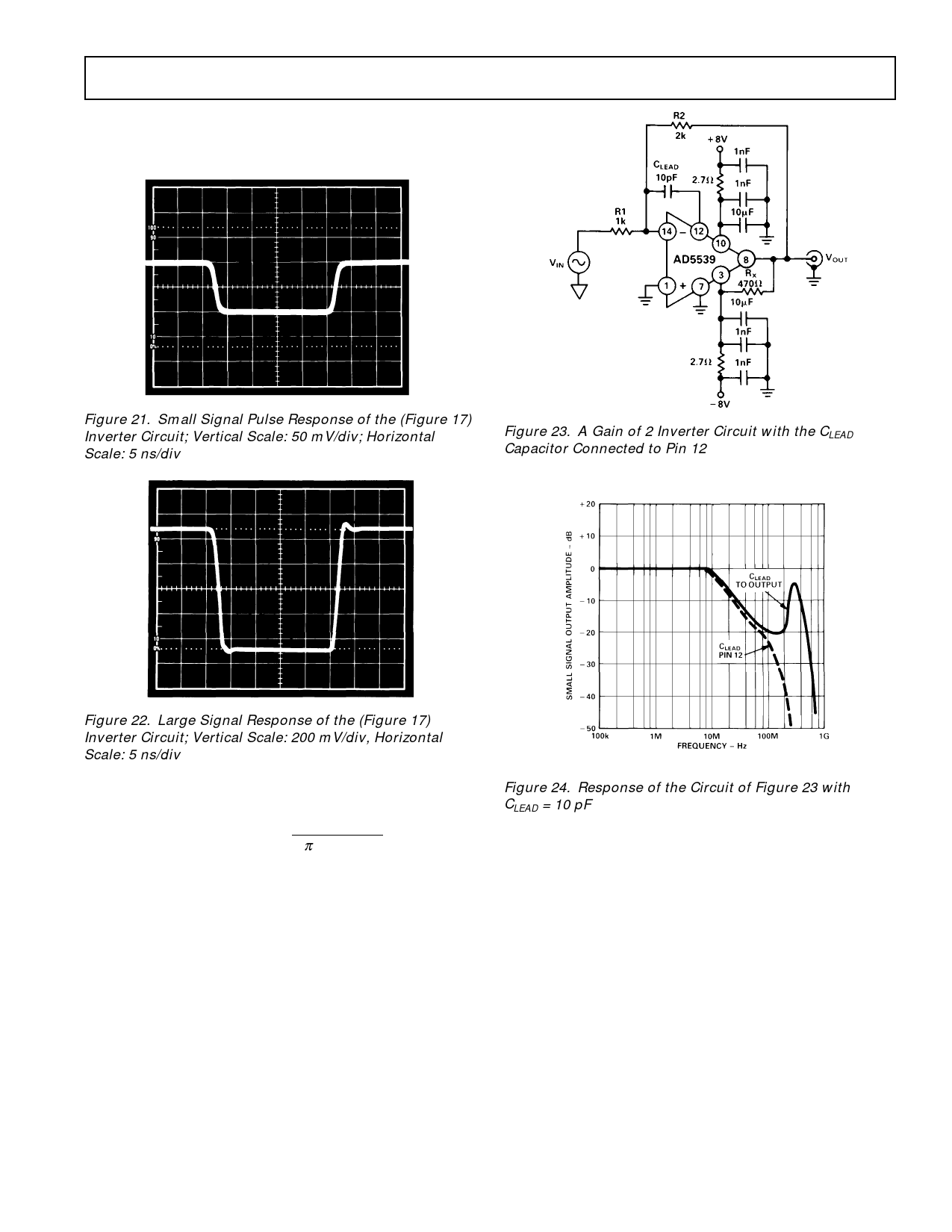
Figures 21 and 22 show the small and large signal pulse re-
sponses of the general purpose inverter circuit of Figure 17, with
CLEAD = 1.5 pF, RLAG = 330 Ω and CLAG = 3.5 pF.
AD5539
Figure 21. Small Signal Pulse Response of the (Figure 17)
Inverter Circuit; Vertical Scale: 50 mV/div; Horizontal
Scale: 5 ns/div
Figure 23. A Gain of 2 Inverter Circuit with the CLEAD
Capacitor Connected to Pin 12
Figure 22. Large Signal Response of the (Figure 17)
Inverter Circuit; Vertical Scale: 200 mV/div, Horizontal
Scale: 5 ns/div
A CLEAD capacitor may be used to limit the circuit bandwidth
and to achieve a single pole response free of overshoot
–3 dB
frequency
=
2π
1
R2 CLEAD
If this option is selected, it is recommended that a CLEAD be
connected between Pin 12 and the summing junction, as shown
in Figure 23. Pin 12 provides a separately buffered version of
the output signal. Connecting the lead capacitor here avoids the
excess output-stage phase shift and subsequent oscillation prob-
lems (at approx. 350 MHz) which would otherwise occur when
using the circuit of Figure 17 with a CLEAD of more than about
2 pF.
Figure 24 shows the response of the circuit of Figure 23 for each
connection of CLEAD. Lag components may also be added to this
circuit to further tailor its response, but, in this case, the results
will be slightly less satisfactory than connecting CLEAD directly
to the output, as was done in Figure 17.
Figure 24. Response of the Circuit of Figure 23 with
CLEAD = 10 pF
A General Purpose Voltage Follower Circuit
Noninverting (voltage follower) circuits pose an additional com-
plication, in that when a lag network is used, the source imped-
ance will affect the noise gain. In addition, the slightly greater
bandwidth of the noninverting configuration makes any excess
phase shift due to the output stage more of a problem.
For example, a gain of 3 noninverting circuit with CLEAD con-
nected normally (across the feedback resistor – Figure 25) will
require a source resistance of 200 Ω or greater to prevent UHF
oscillation; the extra source resistance provides some damping
as well as increasing the noise gain. The frequency response plot
of Figure 26 shows that the highest –3 dB frequency of all the
applications circuits can be achieved using this connection, un-
fortunately, at the expense of a noise gain of 14.2.
REV. B
–9–
Share Link: 