AD590JR-REEL 데이터 시트보기 (PDF) - Analog Devices
부품명
상세내역
제조사
AD590JR-REEL Datasheet PDF : 16 Pages
| |||
AD590
1.6
0.8
0
0.8°C
MAX
–0.8
0.8°C MAX
0.8°C
MAX
–1.6
–55
150
TEMPERATURE (°C)
Figure 9. Nonlinearity
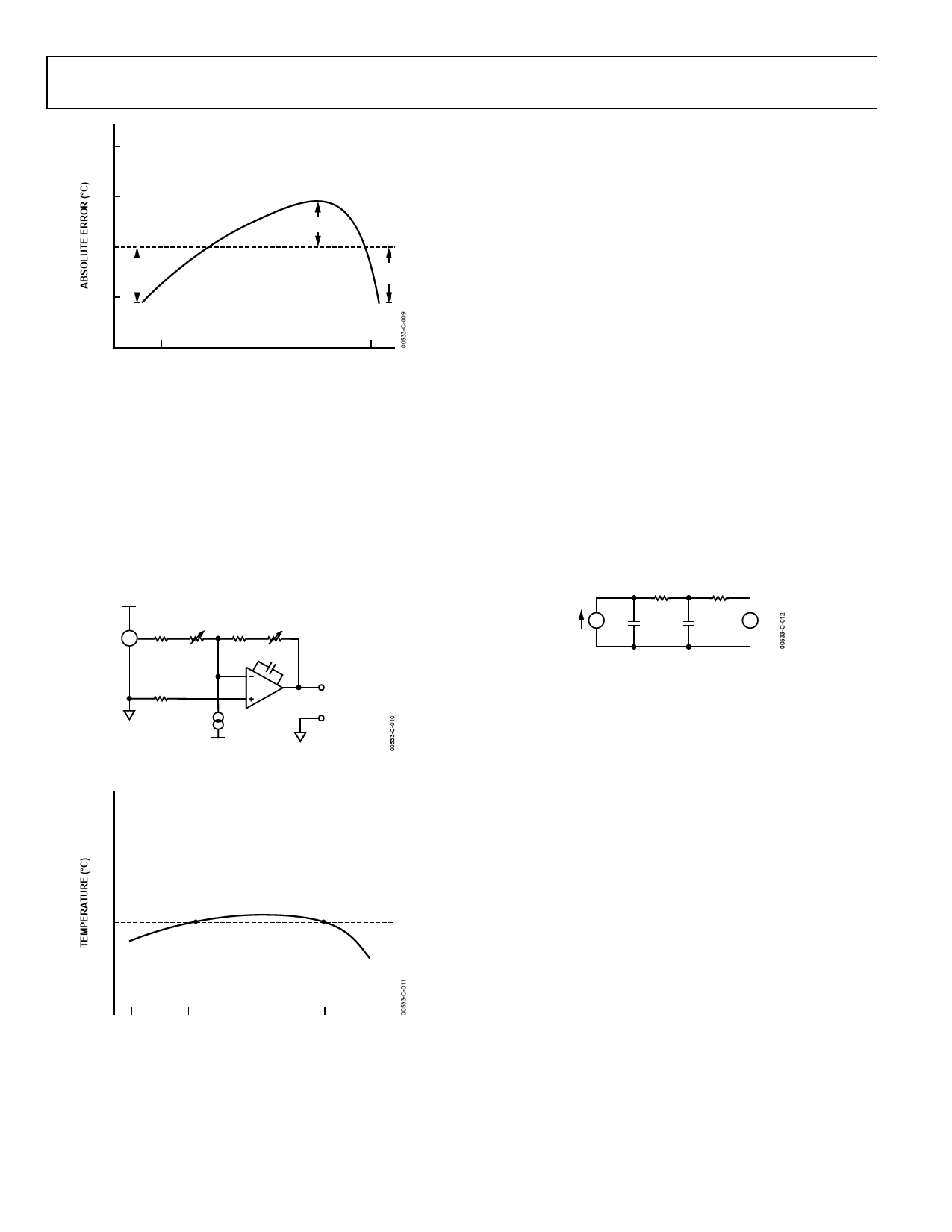
Figure 10 shows a circuit in which the nonlinearity is the major
contributor to error over temperature. The circuit is trimmed by
adjusting R1 for a 0 V output with the AD590 at 0°C. R2 is then
adjusted for 10 V out with the sensor at 100°C. Other pairs of
temperatures may be used with this procedure as long as they
are measured accurately by a reference sensor. Note that for
15 V output (150°C) the V+ of the op amp must be greater than
17 V. Also note that V− should be at least −4 V; if V− is ground,
there is no voltage applied across the device.
15V
AD581
R1
35.7kΩ 2kΩ
R2
97.6kΩ 5kΩ
30pF
27kΩ
AD707A
AD590
V–
100mV/°C
VT = 100mV/°C
Figure 10. 2-Temperature Trim
2
0
–2
–55
0
100
150
TEMPERATURE (°C)
Figure 11. Typical 2-Trim Accuracy
VOLTAGE AND THERMAL ENVIRONMENT EFFECTS
The power supply rejection specifications show the maximum
expected change in output current versus input voltage changes.
The insensitivity of the output to input voltage allows the use of
unregulated supplies. It also means that hundreds of ohms of
resistance (such as a CMOS multiplexer) can be tolerated in
series with the device.
It is important to note that using a supply voltage other than 5 V
does not change the PTAT nature of the AD590. In other words,
this change is equivalent to a calibration error and can be
removed by the scale factor trim (see Figure 8).
The AD590 specifications are guaranteed for use in a low
thermal resistance environment with 5 V across the sensor.
Large changes in the thermal resistance of the sensor’s
environment change the amount of self-heating and result in
changes in the output, which are predictable but not necessarily
desirable.
The thermal environment in which the AD590 is used
determines two important characteristics: the effect of self-
heating and the response of the sensor with time. Figure 12 is a
model of the AD590 that demonstrates these characteristics.
TJ θJC TC θCA
+
P
CCH
CC
TA
–
Figure 12. Thermal Circuit Model
As an example, for the TO-52 package, θJC is the thermal
resistance between the chip and the case, about 26°C/W. θCA is
the thermal resistance between the case and the surroundings
and is determined by the characteristics of the thermal
connection. Power source P represents the power dissipated on
the chip. The rise of the junction temperature, TJ, above the
ambient temperature TA is
( ) TJ − TA = P θ JC + θCA
Equation 1.
Table 4 gives the sum of θJC and θCA for several common
thermal media for both the H and F packages. The heat sink
used was a common clip-on. Using Equation 1, the temperature
rise of an AD590 H package in a stirred bath at 25°C, when
driven with a 5 V supply, is 0.06°C. However, for the same
conditions in still air, the temperature rise is 0.72°C. For a given
supply voltage, the temperature rise varies with the current and
is PTAT. Therefore, if an application circuit is trimmed with the
sensor in the same thermal environment in which it will be
used, the scale factor trim compensates for this effect over the
entire temperature range.
Rev. C | Page 8 of 16
Share Link: 