AD590JRZ-RL 데이터 시트보기 (PDF) - Analog Devices
부품명
상세내역
제조사
AD590JRZ-RL Datasheet PDF : 16 Pages
| |||
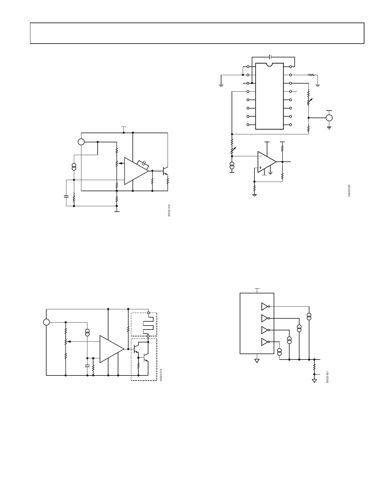
Figure 20 is an example of a current transmitter designed to be
used with 40 V, 1 kΩ systems; it uses its full current range of 4
to 20 mA for a narrow span of measured temperatures. In this
example, the 1 μA/K output of the AD590 is amplified to
1 mA/°C and offset so that 4 mA is equivalent to 17°C and
20 mA is equivalent to 33°C. RT is trimmed for proper reading
at an intermediate reference temperature. With a suitable choice
of resistors, any temperature range within the operating limits
of the AD590 can be chosen.
V+
4mA = 17°C
12mA = 25°C
20mA = 33°C
+ AD581
– VOUT
35.7kΩ
+
RT
AD590
5kΩ
–
0.01µF
10kΩ
12.7kΩ
10Ω
30pF
–
AD707A
+
5kΩ 500Ω
V–
Figure 20. 4 to 20 mA Current Transmitter
Figure 21 is an example of a variable temperature control circuit
(thermostat) using the AD590. RH and RL are selected to set the
high and low limits for RSET. RSET could be a simple pot, a
calibrated multiturn pot, or a switched resistive divider. Powering
the AD590 from the 10 V reference isolates the AD590 from
supply variations while maintaining a reasonable voltage (~7 V)
across it. Capacitor C1 is often needed to filter extraneous noise
from remote sensors. RB is determined by the β of the power
transistor and the current requirements of the load.
V+
V+
AD581
OUT
10V
V–
+
RH AD590
RB
RSET
– 2– 7
LM311
RL
3+ 4
1
C1
10kΩ
HEATING
ELEMENTS
GND
Figure 21. Simple Temperature Control Circuit
Figure 22 shows that the AD590 can be configured with an 8-bit
DAC to produce a digitally controlled setpoint. This particular
circuit operates from 0°C (all inputs high) to 51.0°C (all inputs
low) in 0.2°C steps. The comparator is shown with 1.0°C
hysteresis, which is usually necessary to guard-band for extraneous
noise. Omitting the 5.1 MΩ resistor results in no hysteresis.
AD590
20pF
–15V
DAC OUT
BIT 1
BIT 2
BIT 3
BIT 4
MC
1408/1508
1.25kΩ
REF
+5V
BIT 8
BIT 7
BIT 6
BIT 5
1.15kΩ
200Ω, 15T
+5V
+2.5V
AD580
200Ω
6.98kΩ
+5V +5V
1kΩ, 15T 3
8
+
LM311 7
AD590 2
1
–
4
1kΩ
OUTPUT HIGH-
TEMPERATURE ABOVE SETPOINT
OUTPUT LOW-
TEMPERATURE BELOW SETPOINT
–15V
–15V
5.1MΩ
6.8kΩ
Figure 22. DAC Setpoint
The voltage compliance and the reverse blocking characteristic
of the AD590 allow it to be powered directly from 5 V CMOS
logic. This permits easy multiplexing, switching, or pulsing for
minimum internal heat dissipation. In Figure 23, any AD590
connected to a logic high passes a signal current through the
current measuring circuitry, while those connected to a logic
zero pass insignificant current. The outputs used to drive the
AD590s can be employed for other purposes, but the additional
capacitance due to the AD590 should be taken into account.
5V
CMOS
GATES
+
AD590
+–
+–
+–
–
1kΩ (0.1%)
Figure 23. AD590 Driven from CMOS Logic
Rev. E | Page 11 of 16
Share Link: 