AD7171 데이터 시트보기 (PDF) - Analog Devices
부품명
상세내역
제조사
AD7171 Datasheet PDF : 16 Pages
| |||
AD7171
ADC CIRCUIT INFORMATION
OVERVIEW
The AD7171 is a low power ADC that incorporates a precision
16-bit Σ-∆ modulator and an on-chip digital filter intended for
measuring wide dynamic range, low frequency signals. The device
has an internal clock and one differential input. It operates with
an output data rate of 125 Hz and has a gain of 1. A 2-wire interface
simplifies data retrieval from the AD7171.
FILTER, DATA RATE, AND SETTLING TIME
The AD7171 uses a sinc3 filter. The output data rate is set to 125 Hz;
thus, valid conversions are available every 1/125 = 8 ms. If a reset
occurs, then the user must allow the complete settling time for
the first conversion after the reset. The settling time is equal to
24 ms. Subsequent conversions are available at 125 Hz.
When a step change occurs on the analog input, the AD7171
requires several conversion cycles to generate a valid conversion.
If the step change occurs synchronous to the conversion period,
then the settling time of the AD7171 must be allowed to generate
a valid conversion. If the step change occurs asynchronous to the
end of a conversion, then an extra conversion must be allowed to
generate a valid conversion. The data register is updated with all
the conversions but, for an accurate result, the user must allow
the required time.
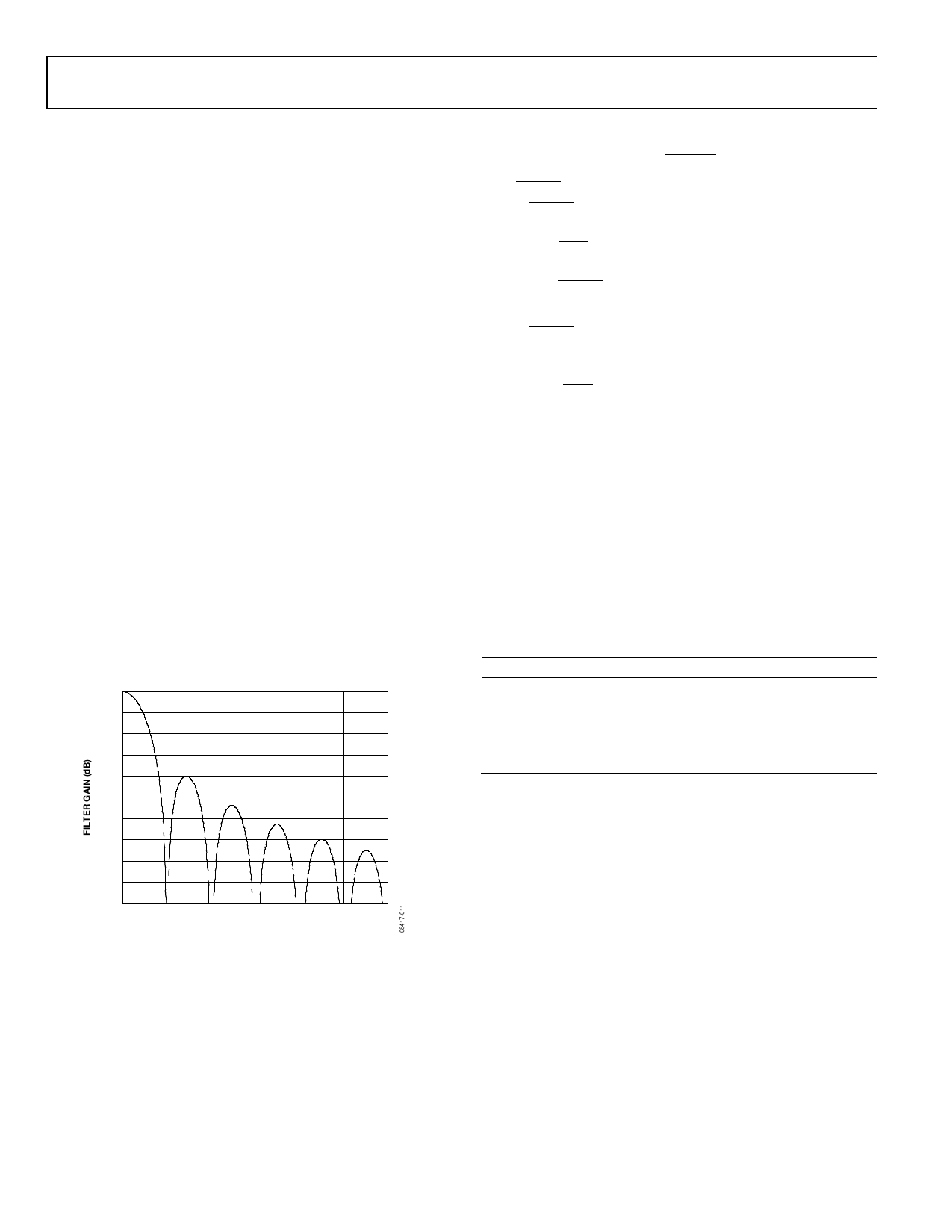
Figure 12 shows the filter response of the filter. The only external
filtering required on the analog inputs is a simple RC filter to
provide rejection at multiples of the master clock. See Table 8
for suitable external RC combinations.
0
–10
–20
–30
–40
–50
–60
–70
–80
–90
–100
0
125
250
375
500
625
750
INPUT SIGNAL FREQUENCY (Hz)
Figure 12. Filter Response
GAIN
The AD7171 has a gain of 1. The acceptable analog input range
is ±VREF. Therefore, with VREF = 5 V, the input range is ±5 V.
Data Sheet
POWER-DOWN/RESET (PDRST)
The PDRST pin functions as a power-down pin and a reset pin.
When PDRST is taken low, the AD7171 is powered down. The
entire ADC is powered down (including the on-chip clock), and
the DOUT/RDY pin is tristated. The circuitry and serial interface
are also reset. This resets the logic, the digital filter, and the analog
modulator. PDRST must be held low for 100 ns minimum to
initiate the reset function (see Figure 4).
When PDRST is taken high, the AD7171 is taken out of power-
down mode. When the on-chip clock has powered up (1 ms,
typically), the modulator then begins sampling the analog input.
The DOUT/RDY pin becomes active, going high until a valid
conversion is available. A reset is automatically performed on
power-up.
ANALOG INPUT CHANNEL
The AD7171 has one differential analog input channel that is
connected to the modulator; that is, the input is unbuffered.
Note that this unbuffered input path provides a dynamic load to
the driving source. Therefore, resistor/capacitor combinations on
the input pins can cause dc gain errors, depending on the output
impedance of the source that is driving the ADC input. Table 8
shows the allowable external resistance/capacitance values such
that no gain error at the 16-bit level is introduced.
Table 8. External RC Combination for No Gain Error
C (pF)
R (Ω)
50
9000
100
6000
500
1500
1000
900
5000
200
The absolute input voltage range is restricted to a range between
GND − 30 mV and VDD + 30 mV. Care must be taken in setting
up the common-mode voltage to avoid exceeding these limits.
Otherwise, there is degradation in linearity and noise performance.
BIPOLAR CONFIGURATION
The AD7171 accepts a bipolar input range. A bipolar input range
does not imply that the device can tolerate negative voltages with
respect to system GND. Signals on the AIN(+) input are referenced
to the voltage on the AIN(−) input. For example, if AIN(−) is 2.5 V,
the analog input range on the AIN(+) input is 0 V to 5 V when a
2.5 V reference is used.
Rev. C | Page 10 of 16
Share Link: 