AD7225(RevB) 데이터 시트보기 (PDF) - Analog Devices
부품명
상세내역
제조사
AD7225 Datasheet PDF : 12 Pages
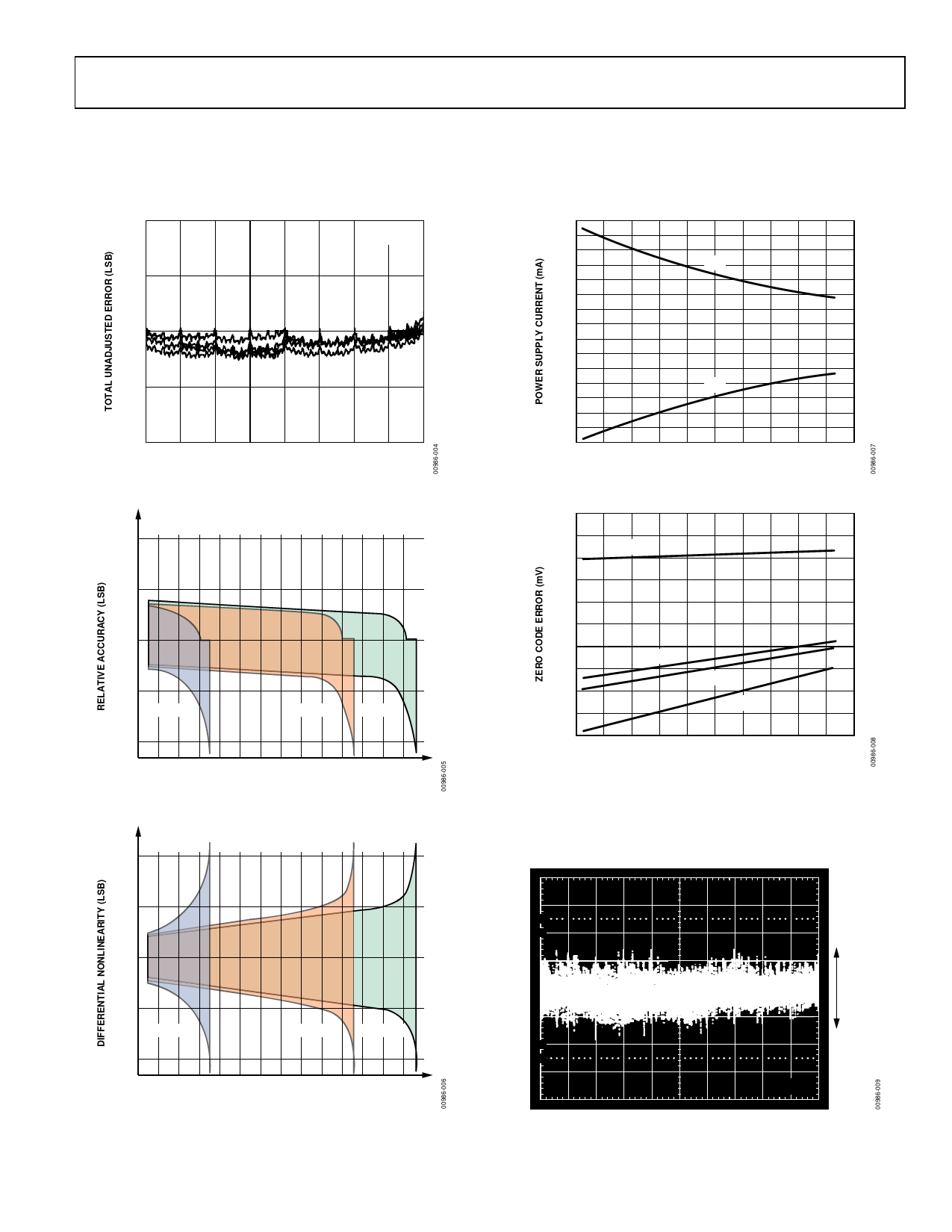
| |||
Only the data held in the DAC register determines the analog
output of the converter. The LDAC signal is common to all four
DACs and controls the transfer of information from the input
registers to the DAC registers. Data is latched into all four DAC
registers simultaneously on the rising edge of LDAC. The
LDAC signal is level triggered and therefore the DAC registers
may be made transparent by tying LDAC LOW (in this case the
outputs of the converters will respond to the data held in their
respective input latches). LDAC is an asynchronous signal and
is independent of WR. This is useful in many applications.
However, in systems where the asynchronous LDAC can occur
during a write cycle (or vice versa) care must be taken to ensure
that incorrect data is not latched through to the output. In other
words, if LDAC is activated prior to the rising edge of WR (or
WR occurs during LDAC), then LDAC must stay LOW for t6
or longer after WR goes HIGH to ensure correct data is latched
through to the output. Table II shows the truth table for AD7225
operation. Figure 9 shows the input control logic for the part
and the write cycle timing diagram is given in Figure 10.
Table II. AD7225 Truth Table
WR LDAC Function
HH
LH
gH
HL
Hg
LL
No Operation. Device not selected
Input Register of Selected DAC Transparent
Input Register of Selected DAC Latched
All Four DAC Registers Transparent
(i.e. Outputs respond to data held in respective
input registers)
Input Registers are Latched
All Four DAC Registers Latched
DAC Registers and Selected Input Register
Transparent Output follows Input Data for
Selected Channel.
GROUND MANAGEMENT AND LAYOUT
Since the AD7225 contains four reference inputs which can be
driven from ac sources (see AC REFERENCE SIGNAL sec-
tion) careful layout and grounding is important to minimize
analog crosstalk between the four channels. The dynamic per-
formance of the four DACs depends upon the optimum choice
of board layout. Figure 11 shows the relationship between input
AD7225
Figure 9. Input Control Logic
Figure 10. Write Cycle Timing Diagram
Figure 11. Channel-to-Channel Isolation
Figure 12. Suggested PCB Layout for AD7225.
Layout Shows Component Side (Top View)
frequency and channel-to-channel isolation. Figure 12 shows a
printed circuit board layout which is aimed at minimizing
crosstalk and feedthrough. The four input signals are screened
by AGND. VREF was limited to between 2 V and 3.24 V to
avoid slew rate limiting effects from the output amplifier during
measurements.
REV. B
–7–
Share Link: 