LH1691 데이터 시트보기 (PDF) - Sharp Electronics
부품명
상세내역
제조사
LH1691 Datasheet PDF : 14 Pages
| |||
LH1691
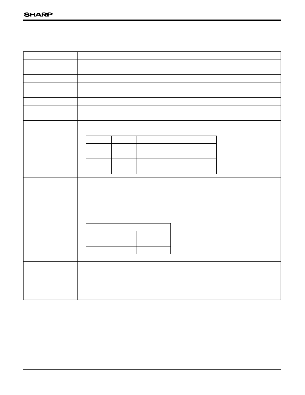
FUNCTIONAL DESCRIPTION
Pin Functions
SYMBOL
VDD
VLS
VCC
VEE
VSS
CKV
SPV
MODE1
MODE2
R/L
CE
TEST1
TEST2
OG1-OG240
FUNCTION
Used as power supply pin for high level LCD drive.
Used as power supply pin for input level shifters.
Used as power supply pin for logic system, normally connected to VSS + 5.0 V.
Used as power supply pin for low level LCD drive.
Used as logic system power supply pin.
Used as vertical shift clock pulse input pin.
Used as vertical scanning start pulse input pin. (At least, input one cycle of CKV during "L"
period of SPV.)
Used as input pins for selecting output mode.
Output mode is set as shown in the table below by setting MODE1 pin and MODE2 pin.
MODE1 MODE2
Output mode
H
H Normal mode (1-pulse scanning)
L
H Continuous 2-pulse mode
H
L
Jumping 2-pulse mode
L
L
Set all outputs to VEE level.
Used as input pin for selecting the shift direction of bi-directional shift register and for
setting the sequence of cascade connection.
LCD drive outputs shift from OG1 to OG240 when set to "H". LCD drive outputs shift from
OG240 to OG1 when set to "L". At the same time, cascade sequence is set as shown in
the table below.
Used as input pin for setting of chip cascade sequence. (Max. 2 cascades)
Cascade sequence
CE
R/L = "H"
R/L = "L"
H
1st
2nd
L
2nd
1st
With above setting, sets the cascade sequence signal inside the IC.
Used as input pins for IC testing.
Must be set to "H".
Used as output pins for LCD drive output, and which output data at 2 levels.
• Selecting data is output at VDD level .
• Non-selecting data is output at VEE level .
4
Share Link: 