AD8148ACPZ-R7 데이터 시트보기 (PDF) - Analog Devices
부품명
상세내역
제조사
AD8148ACPZ-R7 Datasheet PDF : 24 Pages
| |||
AD8146/AD8147/AD8148
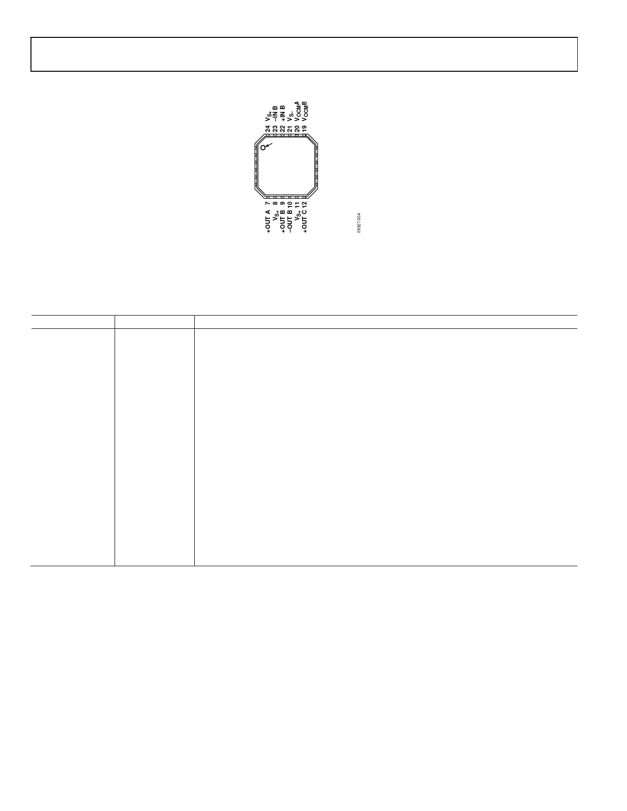
PIN CONFIGURATIONS AND FUNCTION DESCRIPTIONS
OPD 1
VS– 2
–IN A 3
+IN A 4
VS– 5
–OUT A 6
PIN 1
INDICATOR
AD8146
TOP VIEW
(Not to Scale)
18 VOCMC
17 VS+
16 –IN C
15 +IN C
14 VS–
13 –OUT C
Data Sheet
NOTES
1. THE EXPOSED PADDLE ON THE UNDERSIDE OF THE
CHIP MUST BE CONNECTED TO A GROUND PLANE.
Figure 4. AD8146 Pin Configuration
Table 5. AD8146 Pin Function Descriptions
Pin No.
Mnemonic
Description
1
OPD
Output Pull-Down.
2, 5, 14, 21
VS−
Negative Power Supply Voltage.
3
−IN A
Inverting Input, Amplifier A.
4
+IN A
Noninverting Input, Amplifier A.
6
−OUT A
Negative Output, Amplifier A.
7
+OUT A
Positive Output, Amplifier A.
8, 11, 17, 24
VS+
Positive Power Supply Voltage.
9
+OUT B
Positive Output, Amplifier B.
10
−OUT B
Negative Output, Amplifier B.
12
+OUT C
Positive Output, Amplifier C.
13
−OUT C
Negative Output, Amplifier C.
15
+IN C
Noninverting Input, Amplifier C.
16
−IN C
Inverting Input, Amplifier C.
18
VOCMC
The voltage applied to this pin controls output common-mode voltage, Amplifier C.
19
VOCMB
The voltage applied to this pin controls output common-mode voltage, Amplifier B.
20
VOCMA
The voltage applied to this pin controls output common-mode voltage, Amplifier A.
22
+IN B
Noninverting Input, Amplifier B.
23
−IN B
Inverting Input, Amplifier B.
Exposed Paddle GND
Signal Ground Reference.
Rev. B | Page 8 of 24
Share Link: 