AD8517 데이터 시트보기 (PDF) - Analog Devices
부품명
상세내역
제조사
AD8517 Datasheet PDF : 12 Pages
| |||
AD8517/AD8527
Table III. Snubber Network Values for Large Capacitive Loads
CLOAD
680 pF
1 nF
10 nF
Rx
300 Ω
100 Ω
400 Ω
Cx
3 nF
10 nF
30 nF
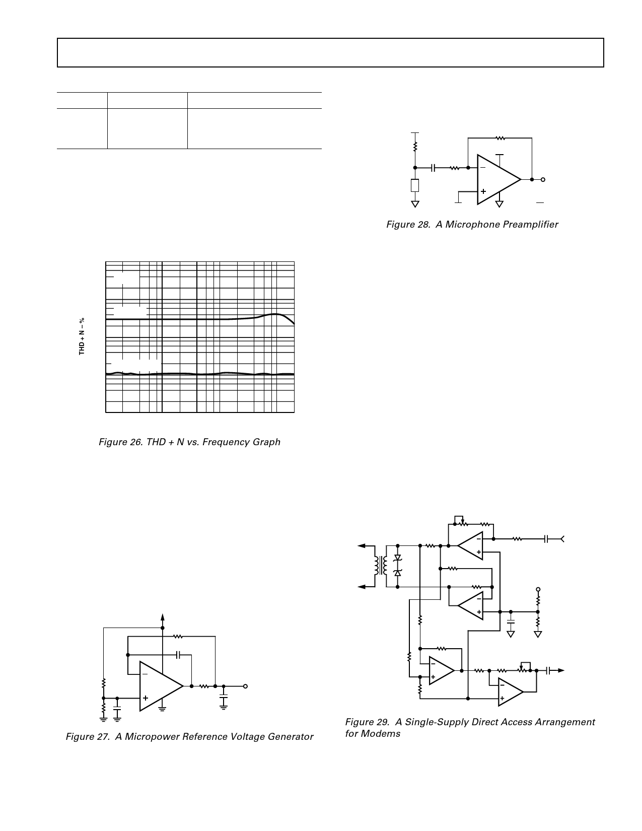
TOTAL HARMONIC DISTORTION + NOISE
The AD85x7 family offers a low total harmonic distortion, which
makes this amplifier ideal for audio applications. Figure 26 shows a
graph of THD + N, for a VS > 3 V the THD + N is about 0.001%
and 0.03% for VS ≥ 1.8 V in a noninverting configuration with a
gain of 1. In an inverting configuration, the noise is 0.003% for
all VSY.
1
AV = +2
0.1
VS = 1.8V
0.01
VS > 3V TO 5V
0.001
0.0001
10
100
1k
FREQUENCY – Hz
10k 20k
Figure 26. THD + N vs. Frequency Graph
A MICROPOWER REFERENCE VOLTAGE GENERATOR
Many single supply circuits are configured with the circuit-biased
to one-half of the supply voltage. In these cases, a false-ground
reference can be created by using a voltage divider buffered by an
amplifier. Figure 27 shows the schematic for such a circuit.
The two 1 MΩ resistors generate the reference voltages while
drawing only 0.9 µA of current from a 1.8 V supply. A capacitor
connected from the inverting terminal to the output of the op
amp provides compensation to allow for a bypass capacitor to be
connected at the reference output. This bypass capacitor helps
establish an ac ground for the reference output.
1.8V TO 5V
10k⍀
0.022F
1M⍀
1M⍀
AD8517
1F
100⍀
VREF
1F 0.9V TO 2.5V
Figure 27. A Micropower Reference Voltage Generator
MICROPHONE PREAMPLIFIER
The AD8517 is ideal to use as a microphone preamplifier.
Figure 28 shows this implementation.
VCC
R1
2.2k⍀
VIN
ELECTRET
MIC
C1
0.1F
R2
22k⍀
VREF
R3
220k⍀
VCC
AD8517
VOUT
| AV |
=
R3
R2
Figure 28. A Microphone Preamplifier
R1 is used to bias an electret microphone and C1 blocks dc
voltage from the amplifier. The magnitude of the gain of the
amplifier is approximately R3/R2 when R2 ≥ 10 × R1. VREF
should be equal to 1/2 1.8 V for maximum voltage swing.
Direct Access Arrangement for Telephone Line Interface
Figure 28 illustrates a 1.8 V transmit/receive telephone line
interface for 600 Ω transmission systems. It allows full duplex
transmission of signals on a transformer-coupled 600 Ω line in a
differential manner. Amplifier A1 provides gain that can be ad-
justed to meet the modem output drive requirements. Both A1
and A2 are configured to apply the largest possible signal on a
single supply to the transformer. Amplifier A3 is configured as a
difference amplifier for two reasons: (1) It prevents the transmit
signal from interfering with the receive signal and (2) it extracts
the receive signal from the transmission line for amplification by
A4. A4’s gain can be adjusted in the same manner as A1’s to
meet the modem’s input signal requirements. Standard resistor
values permit the use of SIP (Single In-line Package) format
resistor arrays. Couple this with the AD8517/AD8527’s 5-lead
SOT-23, 8-lead MSOP, and 8-lead SOIC footprint and this
circuit offers a compact solution.
TO
TELEPHONE
LINE 1:1
ZO
600⍀
T1
MIDCOM
671-8005
P1
Tx GAIN
ADJUST R2
9.09k⍀
R3
2k⍀
2
360⍀
1 A1 3
1/2
6.2V
AD8517
6.2V
R5 R6
10k⍀ 10k⍀
6
7
A2 5
R9
10k⍀
1/2
AD8517
R1
10k⍀
C1
0.1F
+1.8V DC
R7
10k⍀
10F
R8
10k⍀
R10
10k⍀
R11
10k⍀
2
3 A3 1
R12
10k⍀
1/2
AD8527
P2
Rx GAIN
R13 R14 ADJUST
10k⍀ 14.3k⍀
6
2k⍀
7
5 A4
1/2
C2
0.1F
AD8527
TRANSMIT
TxA
RECEIVE
RxA
Figure 29. A Single-Supply Direct Access Arrangement
for Modems
REV. B
–11–
Share Link: 